Type II quantum well mid-infrared optoelectronic devices

a technology of optoelectronic devices and quantum wells, which is applied in the direction of lasers, semiconductor devices, semiconductor lasers, etc., can solve the problems of significant increase in laser packaging costs, inherently high temperature sensitive, and severely affecting the performance of cw (continuous wave)

Active Publication Date: 2005-08-11
WISCONSIN ALUMNI RES FOUND +1
View PDF6 Cites 52 Cited by
  • Summary
  • Abstract
  • Description
  • Claims
  • Application Information

AI Technical Summary

Benefits of technology

[0014] In accordance with the present invention, InP based optoelectronic devices have an active region that includes electron quantum well layers of semiconductor containing nitrogen, such as InAsN or InGaAsN, and a hole layer quantum well of semiconductor containing antimony, such as GaAsSb or InGaAsSb, with a type II structure. The electron quantum well layer may be in tensile or compressive strain and the hole quantum well layer is preferably in compressive strain to provide light generation at desired wavelengths. Light can be generated at relatively long mid-IR wavelengths, e.g., 2-5 μm or higher. A GaInP barrier layer is preferably formed adjacent to the InAsN or InGaAsN layer electron quantum well. The nitrogen content of the electron quantum wells is preferably relatively dilute, for example, 10% or less.

Problems solved by technology

However, conventional InP-based long wavelength diode lasers, at λ=1.3-1.55 μm, are inherently highly temperature sensitive.
This additional temperature controller leads to a significant increase in the laser packaging cost.
However, the strong temperature sensitivity and radiative inefficiency of conventional long-wavelength InP-, InAs-, and GaSb-based lasers severely impacts their CW (continuous wave) performance.
While Quantum Cascade (QC) lasers are available for wavelengths greater than 5 μm, no diode laser sources are currently available which operate CW at room temperature in the 3-5 μm wavelength region.
However, low modal gain, high temperature sensitivity, and poor modulation response are still issues under development by many groups.
Early studies of InGaAsN-active lasers were disappointing in that nitrogen concentrations of 2-3% resulted in poor room temperature PL intensity and very high threshold current density lasers. S. Sato, “Low Threshold and High Characteristics Temperature 1.3 μm Range GaInNAs Lasers Grown by Metalorganic Chemical Vapor Deposition,” Jpn. J. Appl. Phys., Vol. 39, June 2000, pp.
One of the challenges in growing InGaAsN QW lasers by MOCVD is the difficulty of incorporating N into the InGaAs QW, while maintaining a high optical quality film.
These challenges have resulted in difficulties in realizing high performance MOCVD-lnGaAsN QW lasers with AsH3 as the As-precursor until recently.
However, since these studies do not account for the possibility of carrier leakage, the Auger recombination coefficients can be overestimated.
Extending the emission wavelength of InGaAsN-active lasers to 1.55 μm and beyond thus remains a considerable challenge, requiring new active layer materials or new structure designs.
While initial results appear promising, poorer performance, compared with conventional InP-based lasers, remains an issue.
Furthermore, extending the emission wavelengths beyond 1.5 μm with this technology is unlikely due to the high strain of the quantum well employed.

Method used


Image

  • Type II quantum well mid-infrared optoelectronic devices
  • Type II quantum well mid-infrared optoelectronic devices
  • Type II quantum well mid-infrared optoelectronic devices

Examples


Embodiment Construction

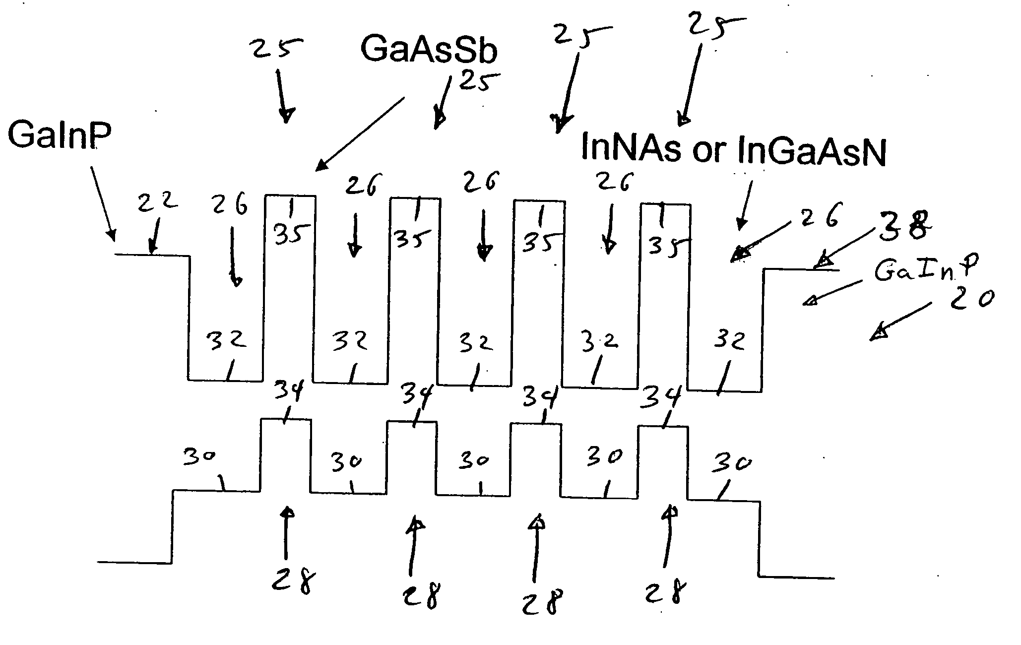
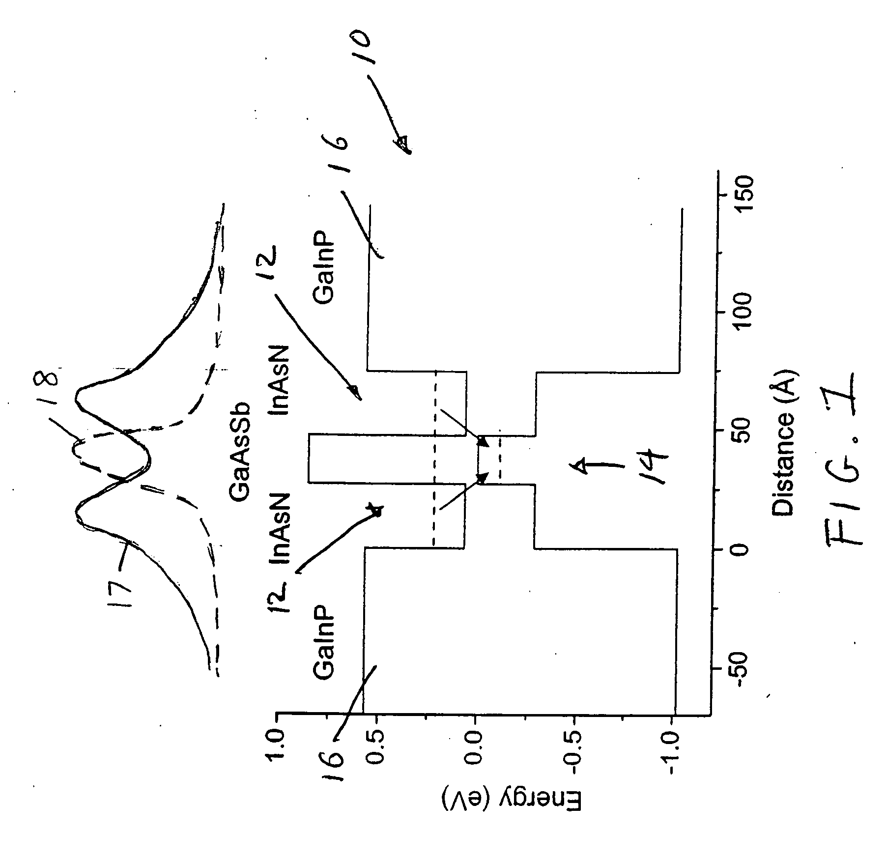
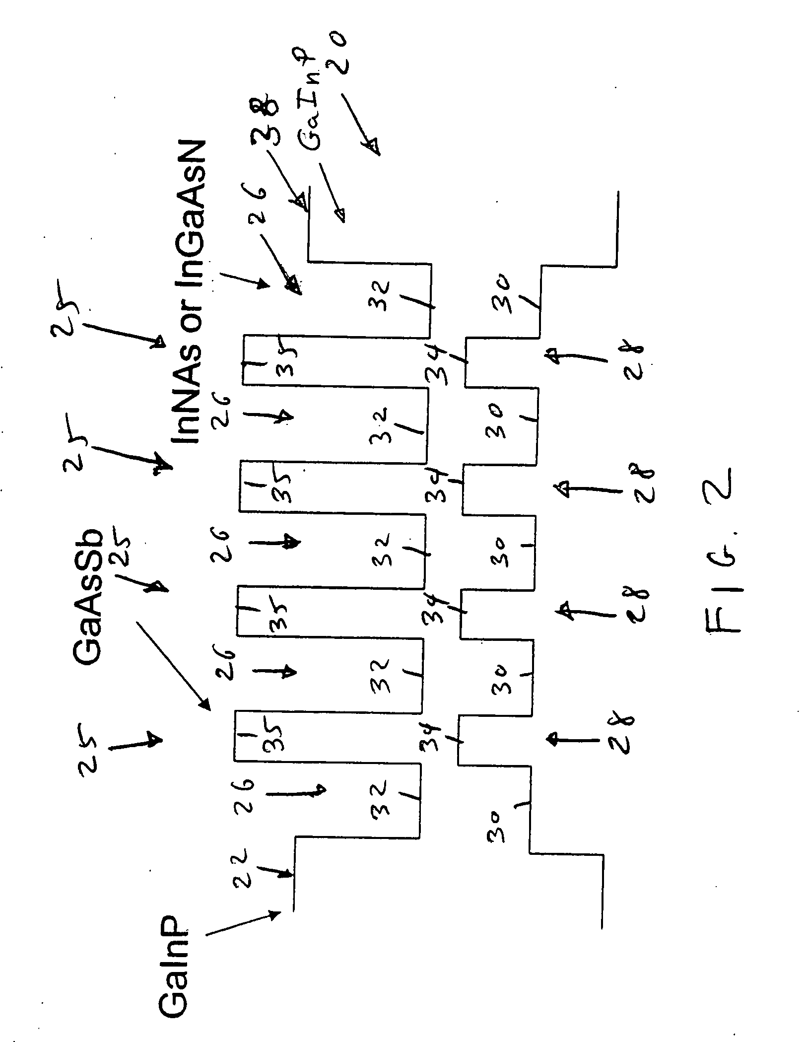
[0026] The present invention provides a novel approach to achieving 2-5 μm lasers and other optoelectronic devices on conventional InP substrates to achieve high-performance, efficient, and room temperature operational sources. The invention utilizes a type-II active region, preferably with multiple-quantum-wells (MQWs) having a modified ‘W’-shape profile, with built-in strain-compensation, strong carrier-confinement, and large electron-hole wave function overlap.

[0027] In accordance with the invention, rather than employing type-I InGaAsN quantum wells (QWs) with high N-content, longer wavelengths may be accessed more readily via type-II InAsN / GaAsSb or InGaAsN / GaAsSb structures. The energy gap in a type-II structure is governed primarily by the relative conduction and valence band alignments in the two adjacent layers rather than by the bulk gap in a single layer. The resulting flexibility comes at the expense of reduced overlap between the electron and hole wave functions that n...


PUM


Abstract

Semiconductor optoelectronic devices such as diode lasers are formed on InP substrates with an active region with an InAsN or InGaAsN electron quantum well layer and a GaAsSb or InGaAsSb hole quantum well layer which form a type II quantum well. The active region may be incorporated in various devices to provide light emission at relatively long wavelengths, including light emitting diodes, amplifiers, surface emitting lasers and edge-emitting lasers.

Description

STATEMENT OF GOVERNMENT RIGHTS [0001] This invention was made with United States Government support awarded by the following agency: NSF 0139823. The United States Government has certain rights in this invention.FIELD OF THE INVENTION [0002] The present invention relates generally to the field of optoelectronic devices such as light emitting diodes and semiconductor diode lasers and more specifically to the field of type II quantum well devices. BACKGROUND OF THE INVENTION [0003] Fiber optic transmission of data signals across large distances is presently accomplished using a variety of laser transmitters, which generally operate at near-infrared and infrared (IR) wavelengths. [0004] 1.3 μm in-plane (edge-emitting) lasers or vertical cavity surface emitting lasers (VCSELs) operating at a modulation bandwidth of 10 Gb / s, for the metro application using single-mode fiber, will allow data transmission up to a distance of 20-30 km. J. S. Harris, Jr., “Tunable Long-Wavelength Vertical-Ca...

Claims


Application Information

Patent Timeline
Patent Type & Authority Applications(United States)
IPC IPC(8): H01L21/00H01L29/06H01L33/06H01L33/26H01L33/32H01S5/028H01S5/183H01S5/22H01S5/223H01S5/34H01S5/343
CPCB82Y20/00H01S2304/04H01L33/26H01L33/32H01S5/028H01S5/18311H01S5/2224H01S5/2226H01S5/2231H01S5/3406H01S5/3422H01S5/3425H01S5/34306H01S5/3436H01L33/06
Inventor MAWST, LUKE J.TANSU, NELSONMEYER, JERRY R.VURGAFTMAN, IGOR
Owner WISCONSIN ALUMNI RES FOUND
Why Eureka
Try Eureka