Tapered structure for providing coupling between external optical device and planar optical waveguide and method of forming the same

a tapered coupling and external optical device technology, applied in the direction of optical waveguide light guide, instruments, optics, etc., can solve the problems of inability to monolithically integrate light sources with the remaining components of the opto-electronic platform, inability to use edge coupling techniques with relatively thin, sub-micron dimensioned silicon waveguides, and inability to achieve dimensional accuracy and slope control

Active Publication Date: 2005-08-11
CISCO TECH INC
View PDF4 Cites 28 Cited by
  • Summary
  • Abstract
  • Description
  • Claims
  • Application Information

AI Technical Summary

Benefits of technology

[0014] In accordance with the present invention, the formation of a tapered evanescent coupling region is based on using gray-scale lithography to obtain the controlled slope and dimensional accuracy required for forming the desired tapered region for providing efficient coupling between external optics and a relatively thin silicon optical waveguide layer in an SOI wafer.
[0015] Various embodiments of the present invention illustratively form both coupling optics and the tapered evanescent coupling region in the same substrate. In certain embodiments, a tapered region of low refractive index material (e.g., an oxide) is formed along a first major surface of a silicon substrate, with the opposing major surface processed using masks and etching techniques to form angled surfaces appropriate for coupling a free space optical signal into the evanescent coupling region. Advantageously, cavity regions may also be formed in the coupling substrate to prevent the premature re-entry of light from the optical waveguide into the coupling substrate.

Problems solved by technology

In addition, the material costs of silicon-based devices are considerably lower than those for competing technologies, such as gallium arsenide or indium phosphide.
At the present time, it is not possible to monolithically integrate light sources with the remaining components on the opto-electronic platform, since silicon-based lasers and light emitting diodes (LEDs) are only now beginning to be developed.
Therefore, it is clear that this edge coupling technique is not readily applicable for use with relatively thin, sub-micron dimensioned silicon waveguides.
As direct coupling in the above-described manner does not provide a sufficiently small spot size, alternative techniques to transfer light into a silicon waveguide have been developed.
To date, however, there are no known manufacturing methods or processes of producing precision input / output wafer structures with tapered evanescent coupling regions.

Method used


Image

  • Tapered structure for providing coupling between external optical device and planar optical waveguide and method of forming the same
  • Tapered structure for providing coupling between external optical device and planar optical waveguide and method of forming the same
  • Tapered structure for providing coupling between external optical device and planar optical waveguide and method of forming the same

Examples


Embodiment Construction

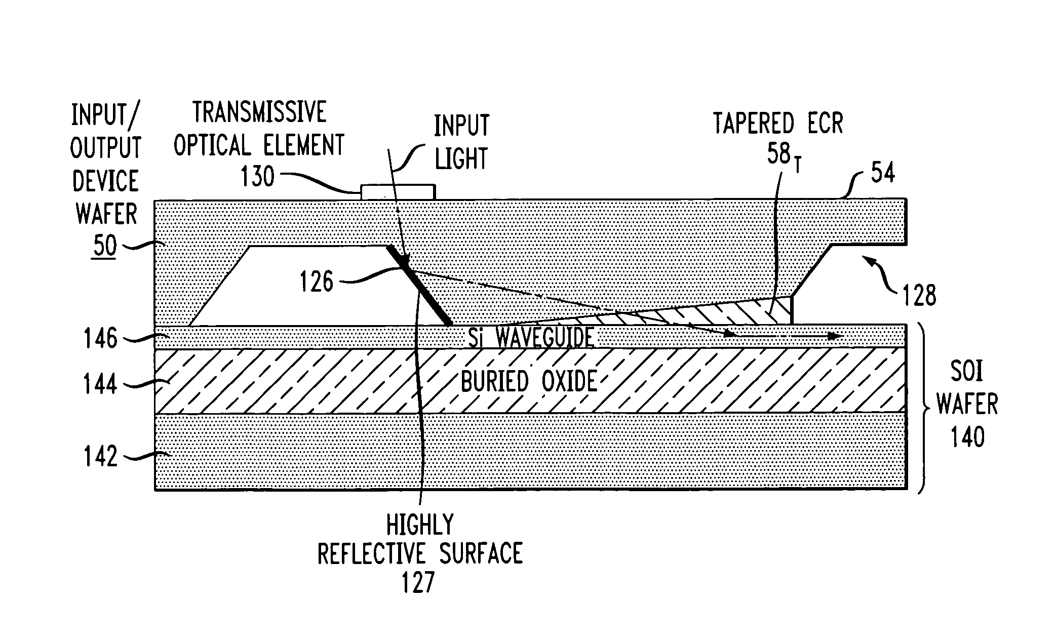
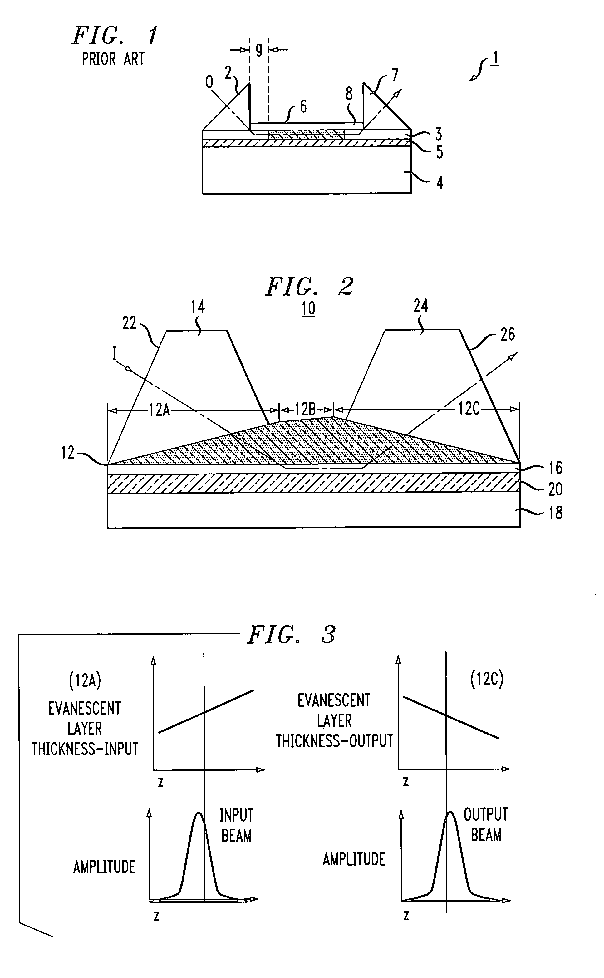
[0027]FIG. 2 illustrates, in a cut-away partial view, an exemplary arrangement 10 of the present invention utilizing a tapered evanescent coupling region 12 disposed between an external optical coupling element 14 (in this case, a prism) and a relatively thin silicon optical waveguide layer 16. In the particular embodiment of FIG. 2, silicon waveguide layer 16 is formed as part of an SOI structure, the SOI structure further comprising a silicon substrate 18 and buried oxide layer 20. As shown in FIG. 2, buried oxide layer 20 is disposed between the relatively thin upper silicon optical waveguide layer 16 and silicon substrate 18. In the utilization of arrangement 10, a light beam I is introduced from an external source (not shown) and impinges an input coupling facet 22 of input prism 14. The light beam is thereafter refracted at the proper angle through prism 14, passes through tapered evanescent coupling region 12 and enters silicon optical waveguide layer 16.

[0028] In order for ...


PUM


Abstract

Methods of forming a tapered evanescent coupling region for use with a relatively thin silicon optical waveguide formed with, for example, an SOI structure. A tapered evanescent coupling region is formed in a silicon substrate that is used as a coupling substrate, the coupling substrate thereafter joined to the SOI structure. A gray-scale photolithography process is used to define a tapered region in photoresist, the tapered pattern thereafter transferred into the silicon substrate. A material exhibiting a lower refractive index than the silicon optical waveguide layer (e.g., silicon dioxide) is then used to fill the tapered opening in the substrate. Advantageously, conventional silicon processing steps may be used to form coupling facets in the silicon substrate (i.e., angled surfaces, V-grooves) in an appropriate relation to the tapered evanescent coupling region. The coupling facets may be formed contiguous with the tapered evanescent coupling region, or formed through the opposing side of the silicon substrate.

Description

TECHNICAL FIELD [0001] The present invention relates to the formation and utilization of a tapered coupling region between an external optical coupling device (such as a prism) and a planar optical waveguide, such as a waveguide formed in an upper silicon layer of a Silicon-On-Insulator (SOI) wafer structure. BACKGROUND OF THE INVENTION [0002] It has been recognized for some time that most of the integrated circuit devices, processes and techniques that revolutionized the electronics industry can be adapted to produce optoelectronic integrated circuits. Due to the dominance of silicon as the material of choice for electronic circuits, the use of silicon-based optoelectronic integrated circuit platforms is highly desirable. In many of today's optoelectronic circuit arrangements, a Silicon-On-Insulator (SOI) wafer is utilized as the platform, with one or more silicon waveguides being formed in the upper silicon layer of the SOI structure. These high-index contrast silicon waveguides (...

Claims


Application Information

Patent Timeline
Patent Type & Authority Applications(United States)
IPC IPC(8): G02B6/10G02B6/34G02B6/42
CPCG02B6/34G02B6/4214G02B6/42
Inventor PATEL, VIPULKUMAR KANTILALGOTHOSKAR, PRAKASHMONTGOMERY, ROBERT KEITHGHIRON, MARGARET
Owner CISCO TECH INC
Why Eureka
Try Eureka