Semiconductor device and method for fabricating the same

Inactive Publication Date: 2005-08-18
COLLABO INNOVATIONS INC
View PDF11 Cites 13 Cited by
  • Summary
  • Abstract
  • Description
  • Claims
  • Application Information

AI Technical Summary

Benefits of technology

[0020] As described above, according to the semiconductor device and the fabrication method thereof in the present invention, a semiconductor device can be provided in which the punch-through immunity is enhanced and the controllable range of the threshold voltage is

Problems solved by technology

For example, IGBTs having the trench gate structure have both a high-input impedance characteristic of a MISFET and a low saturation voltage characteristic of a bipolar transistor, and therefore, are utilized extensively in uninterruptible power source devices,

Method used


Image

  • Semiconductor device and method for fabricating the same
  • Semiconductor device and method for fabricating the same
  • Semiconductor device and method for fabricating the same

Examples


first embodiment

[0030] (First Embodiment)

[0031]—Construction of Semiconductor Device—

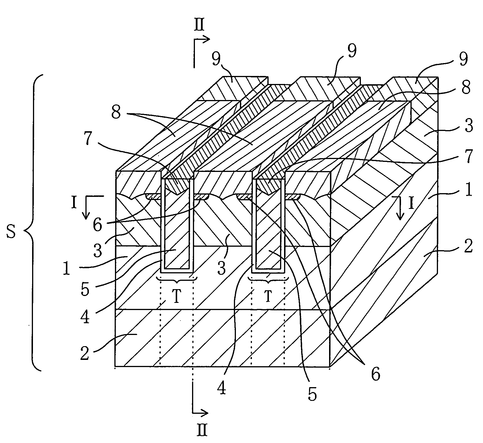
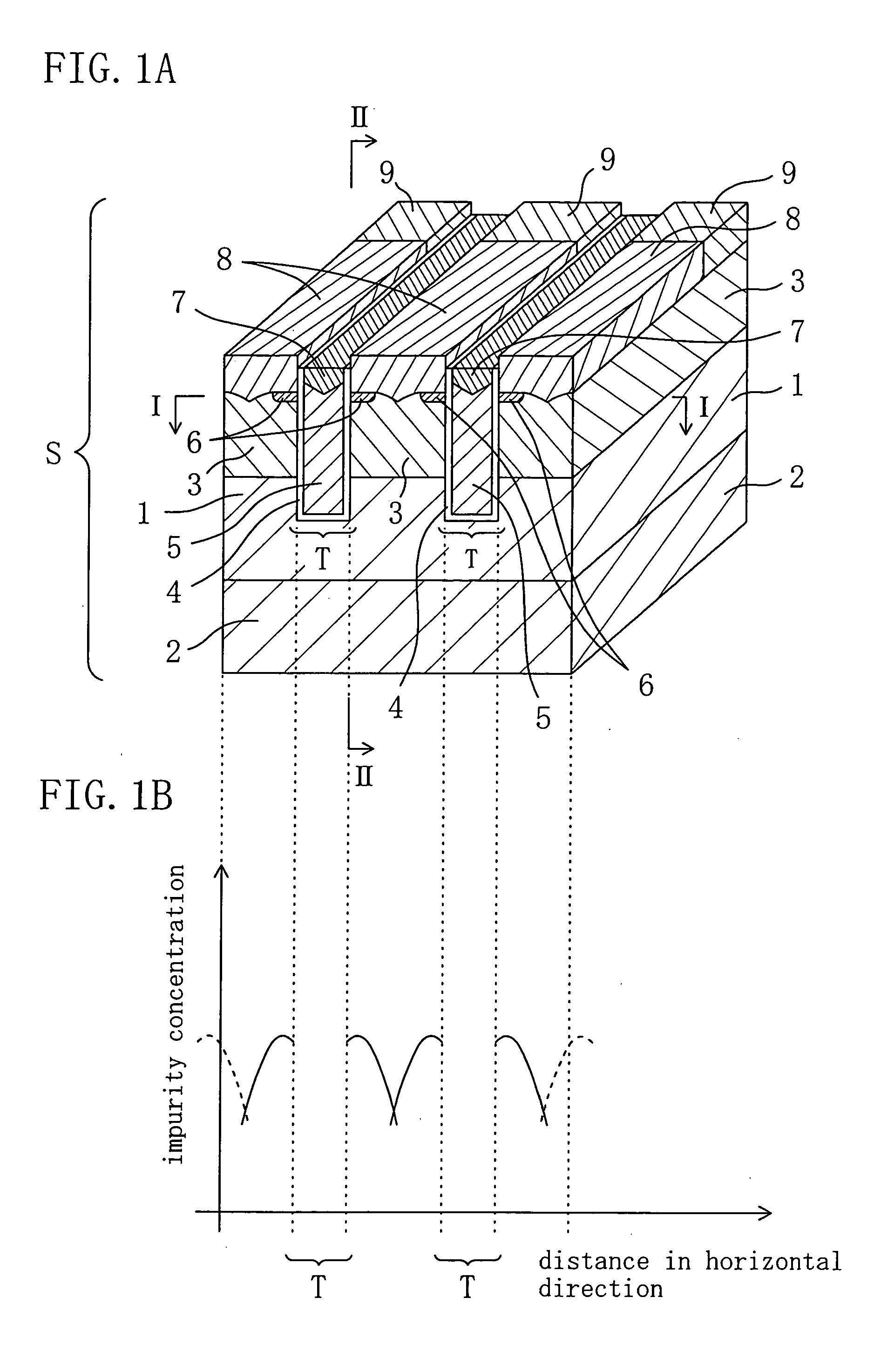
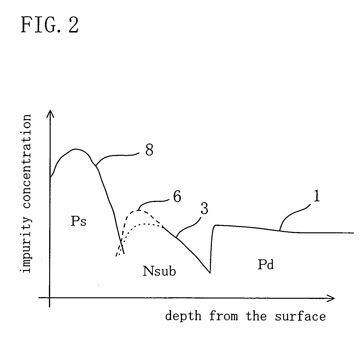
[0032]FIG. 1A and FIG. 1B are a perspective view showing a construction of a semiconductor device having a trench gate structure according to the first embodiment and a graph illustrating impurity concentration profile in a section taken along the line I-I, respectively. Wherein, a silicide layer 10 in FIG. 4C is not shown in FIG. 1A for the sake of simplification of the construction.

[0033] As shown in FIG. 1A, the semiconductor device in the present embodiment includes: a high concentration P-type drain region 2 formed in a silicon substrate S; a low concentration P-type drain region (EPI) 1 formed on the high concentration P-type drain region 2; a high concentration P-type source region 8 formed over the low concentration drain region 1; and a N-type substrate region 3 formed between the high concentration P-type source region 8 and the low concentration P-type drain region (EPI) 1. Trenches T for gate electrode...

second embodiment

[0052] (Second Embodiment)

[0053]—Construction of Semiconductor Device—

[0054]FIG. 6A and FIG. 6B are a perspective view showing a semiconductor device having a trench gate structure according to the second embodiment and a graph illustrating impurity concentration profile in a section taken along the line VI-VI, respectively. Wherein, a silicide layer 10 in FIG. 5C is not shown in FIG. 6A for the sake of simplification of the structure. The construction of the semiconductor device of the present embodiment is basically the same as that in the first embodiment (see FIG. 1A), except the N-type pocket region 6, and description of the members having the same structures is omitted.

[0055] As shown in FIG. 6A, a N-type pocket region 6B is formed entirely in a region between the N-type substrate region 3 and the high concentration P-type source region 8 in the semiconductor device of the present embodiment. Namely, one of the significant features of the semiconductor device of the present e...


PUM


Abstract

A semiconductor device includes: a semiconductor substrate; a first semiconductor region formed in the reverse surface region of the semiconductor substrate and including a first conductivity type impurity; a second semiconductor region formed on the first semiconductor region in the semiconductor substrate and including a second conductivity type impurity; a third semiconductor region formed on the second semiconductor region in the semiconductor substrate and including a first conductivity type impurity; a trench passing through the second and third semiconductor regions and reaching the first semiconductor region; and a gate insulating film formed along the wall face of the trench; a gate electrode formed on the gate insulating film in the trench. Further, a pocket region including a second conductivity type impurity of which peak concentration is higher than that of the second semiconductor region is formed by a side of the trench between the second semiconductor region and the third semiconductor region.

Description

CROSS REFERENCE TO RELATED APPLICATIONS [0001] This Non-provisional application claims priority under 35 U.S.C. §119(a) on Patent Application No. 2004-038878 filed in Japan on Feb. 16, 2004, the entire contents of which are hereby incorporated by reference. [0002] 1. Field of the Invention [0003] The present invention relates to a semiconductor device having a trench MIS (Metal-Insulator-Semiconductor) gate structure and a method for fabricating the same. [0004] 2. Background of the Invention [0005] Conventionally, a trench gate structure in which a trench is formed in a semiconductor substrate and a gate electrode is buried in the trench is employed in semiconductor devices such as IGBTs (Insulated Gate Bipolar Transistor), MISFETs (Field Effect Transistor), and is advantageous in application to power sources and the like. For example, IGBTs having the trench gate structure have both a high-input impedance characteristic of a MISFET and a low saturation voltage characteristic of a ...

Claims


Application Information

Patent Timeline
IPC IPC(8): H01L29/78H01L21/265H01L21/331H01L21/336H01L29/10H01L29/43H01L29/45H01L29/739
CPCH01L21/26586H01L29/1095H01L29/456H01L29/7813H01L29/66734H01L29/7397H01L29/66348
Inventor MIYATA, SATOEMIZOKUCHI, SHUJI
Owner COLLABO INNOVATIONS INC
Why Eureka
Try Eureka