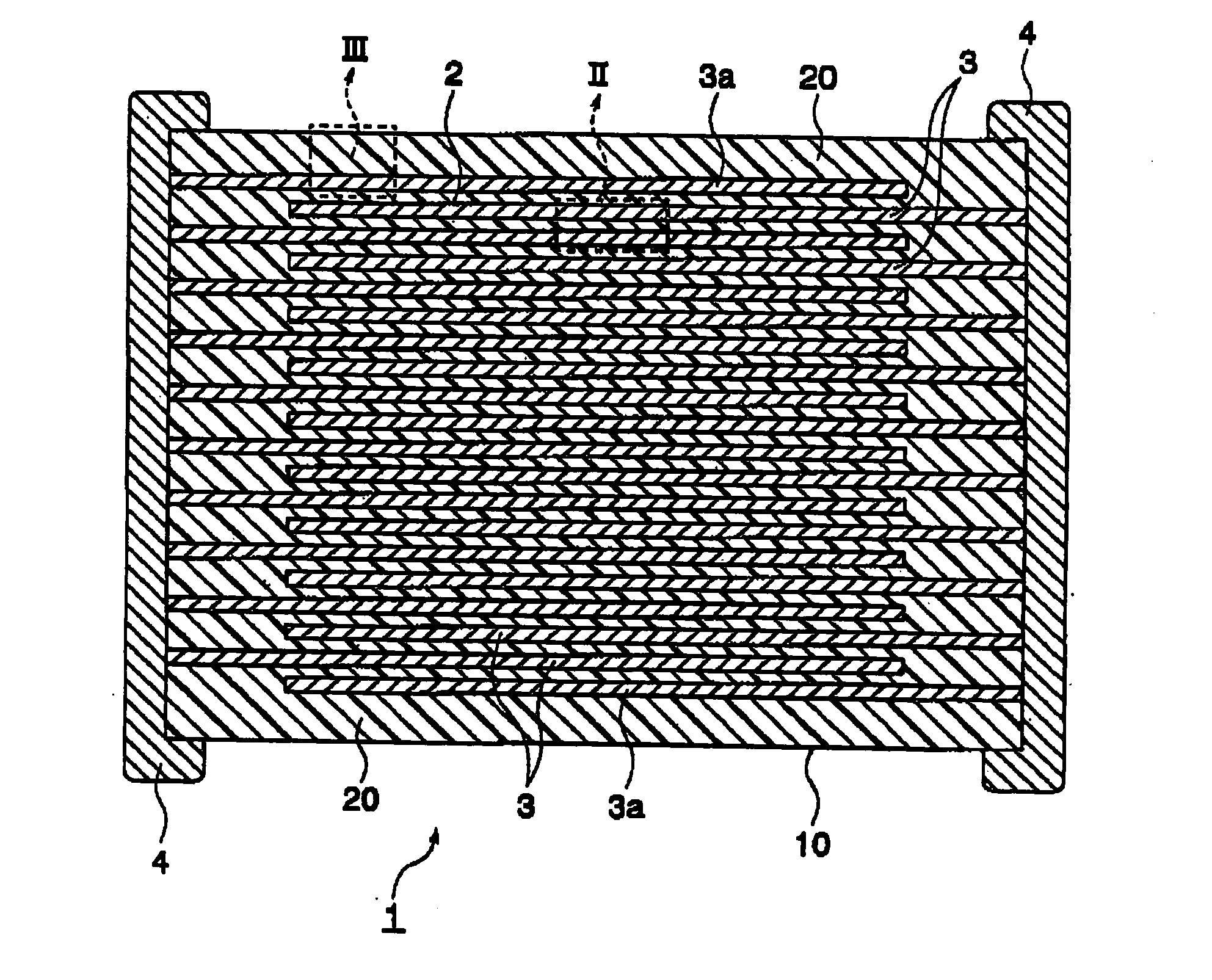
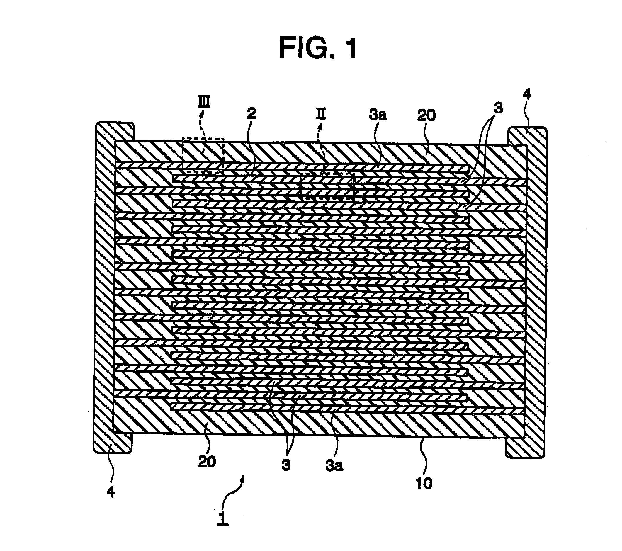
Multilayer ceramic capacitor
a multi-layer ceramic and capacitor technology, applied in the direction of fixed capacitors, fixed capacitor details, wheelchairs/patients, etc., can solve the problems of deterioration of all kinds of electric characteristics (tan , bias characteristic, temperature characteristic, reliability, etc., and achieve the effect of improving tc bias characteristic and all kinds of electric characteristics
- Summary
- Abstract
- Description
- Claims
- Application Information
AI Technical Summary
Benefits of technology
Problems solved by technology
Method used
Image

Examples
example 1
[0128] Preparing Dielectric Layer Paste
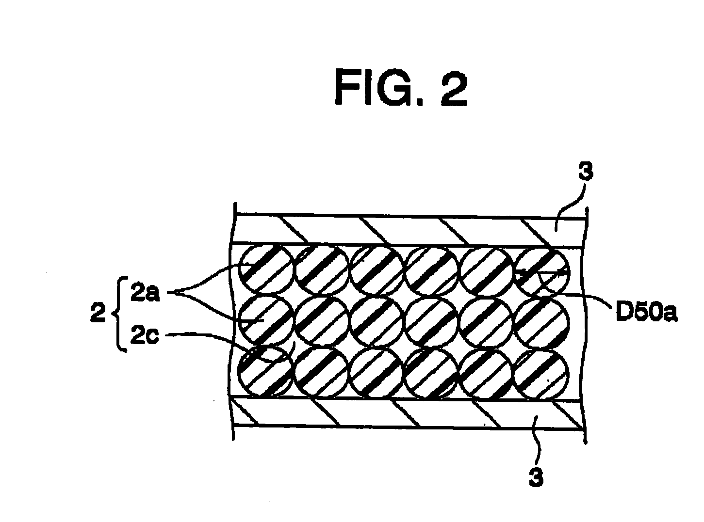
[0129] First, as dielectric material, PVB(polyvinyl butyral) resin as binder, DOP(dioctyl phthalate) as plasticizer, and ethanol as solvent were prepared. Dielectric material was produced by preparing a plural kind of BaTiO3 having average particle size D50c of 0.2 μm as main component, and for each BaTiO3, 0.2 mole % of MnCO3, 0.5 mole % of MgO, 0.3 mole % of V2O, 2 mole % of Y23, 3 mole % of CaCO3, 3 mole % of BaCO3, 3 mole % of SiOas subcomponent were prepared and wet mixed for 16 hours in the ball mill and dried.
[0130] Next, compared with the dielectric material, 10 wt % of binder, 5 wt % of plasticizer, 150 wt % of solvent were weighed, mixed by ball mill, and slurrying was performed to obtain dielectric layer paste.
Preparing Internal Electrode Layer Paste
[0131] Ni particles having average particle size of 0.4 μm as conductive material, dielectric material for additives, ethyl cellulose resin as binder, and terpineol as solvent were p...
example 2
[0160] Capacitor samples ware manufactured in the same way as example 1, except the thickness of internal dielectric layer 2 was varied to 1.9 μm, 1.7 μm, 1.5 μm, and 0.9 μm, and evaluated in the same way as example 1, then, the same results were obtained.
reference example 1
[0161] Capacitor samples were manufactured in the same way as example 1, except the thickness of internal dielectric layer 2 was varied to 2.0 μm and 2.2 μm and evaluated in the same way as example 1.
[0162] As a result, when the thickness of internal dielectric layer 2 was at least 2 μm, particle growth in dielectric layer was hardly seen due to the small effect of dielectric material for additives and that an average particle size of dielectric particles in internal dielectric layer 2 was almost constant and was not effected by ceramic particles (dielectric material for additives) in internal electrode layer.
PUM
| Property | Measurement | Unit |
|---|---|---|
| thickness | aaaaa | aaaaa |
| particle size | aaaaa | aaaaa |
| thickness | aaaaa | aaaaa |
Abstract
Description
Claims
Application Information
 - R&D Engineer
- R&D Manager
- IP Professional
- Industry Leading Data Capabilities
- Powerful AI technology
- Patent DNA Extraction
Browse by: Latest US Patents, China's latest patents, Technical Efficacy Thesaurus, Application Domain, Technology Topic.
© 2024 PatSnap. All rights reserved.Legal|Privacy policy|Modern Slavery Act Transparency Statement|Sitemap