Method of fabricating passivation layer for organic devices

a technology of organic devices and passivation layers, which is applied in the direction of semiconductor devices, basic electric elements, electrical equipment, etc., can solve the problems of short life, fast deterioration of devices, and easy deterioration of organic devices, and achieves the effect of weak heat resistance and easy deterioration

Inactive Publication Date: 2005-08-18
ELECTRONICS & TELECOMM RES INST
View PDF9 Cites 458 Cited by
  • Summary
  • Abstract
  • Description
  • Claims
  • Application Information

AI Technical Summary

Benefits of technology

[0012] The present invention provides a method of fabricating very dense passivation layers of organic devices that are weak to heat and easily deteriorated due to moisture and oxygen.

Problems solved by technology

Although there is a difference depending on a material of which such an OLED is formed, the device is deteriorated fast and thus has a short lifetime.
The dark spot is more greatly expanded during the operation of the OLED device and continuously deteriorates the organic device even during keeping in the normal environment.
In particular, external oxygen and moisture fatally affect the lifetime of the organic device.
The organic materials consisting organic transistors are easily degraded due to the reaction with external oxygen and moisture.
Thus, the improvement of the lifetime of the organic devices such as organic transistors and OLEDs and a passivation layer for passivating the organic devices from moisture and oxygen accelerating the expansion of the dark spots have been become a great issue in the early stage of developing the organic devices.
However, such SUS metal lid type-encapsulation bears a heavy price burden, and is opaque and inflexible and thus cannot be used in top-emission OLEDs and flexible displays.
However, according to the results of experiments that was performed using an inorganic thin film such as SiOx, SiNx, or the like, a single layer cannot sufficiently passitvate an organic device and the characteristics of a multilayer inorganic and / or organic thin films are not satisfactory.
Then, the substrate or the devices sensitive to heat should be deformed and deteriorated.
On the other hand, with physical deposition methods such as e-beam evaporation and thermal evaporation, step coverage of the thin film passivation layers is not good, and the density of the thin film type passivation layer is not dense enough to protect the devices from the permeation of gases.
Conventional sputter deposition method also results in substrate deformation due to plasma induced-surface heating of organic devices or plastic substrate.

Method used


Image

  • Method of fabricating passivation layer for organic devices
  • Method of fabricating passivation layer for organic devices
  • Method of fabricating passivation layer for organic devices

Examples


experimental example

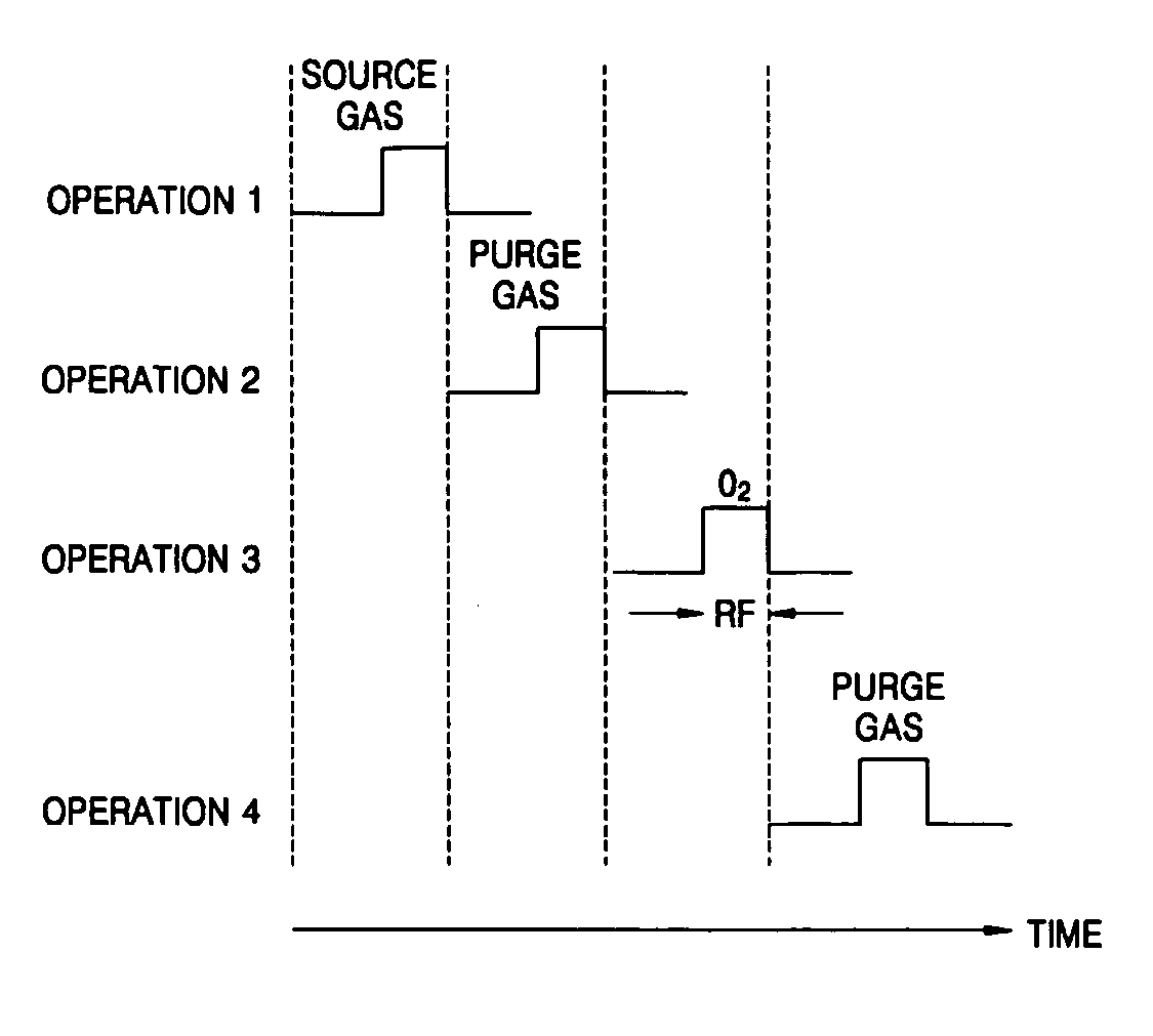
[0048] An OLED including an anode formed of ITO and a cathode formed of Al was formed on a glass substrate. A hole transfer layer, a fluorescent layer, and an electron transfer layer of the OLED are deposited as a NPB (600 Å) / Alq3 (600 Å) / LiF (10 Å) structure using a vacuum deposition apparatus. An Al2O3:N thin film is deposited on the OLED to a thickness of 100 to 300 nm at a temperature between 40° C. and 80° C. using pulsed plasma enhanced atomic layer deposition. The difference of thickness in the range of 100 to 300 nm did not show any considerable differences in the results. The 40° C.-passivation layer also showed the same result as the 60° C.-passivation layer. FIG. 10 is view illustrating lifetime curves of an OLED with a 300 nm thick-passivation layer and an OLED not including a passivation layer.

[0049] When the plasma pulse time was 0.5 s and the substrate temperature was 40, 60, and 80° C., the maximum temperature during the deposition process of a 300 nm thick-film was...


PUM

PropertyMeasurementUnit
temperatureaaaaaaaaaa
thicknessaaaaaaaaaa
thicknessaaaaaaaaaa

Abstract

Provided is a method of fabricating a passivation layer for an organic device, including: forming the organic device on a substrate; and forming a passivation layer on the organic device. Here, forming the passivation layer on the organic device includes forming an inorganic thin film by thin film deposition using pulsed plasma.

Description

BACKGROUND OF THE INVENTION [0001] This application claims the priority of Korean Patent Application No. 10-2004-0010402, filed on Feb. 17, 2004, and No. 10-2005-0012453, filed on Feb. 15, 2005 in the Korean Intellectual Property Office, the disclosures of which are incorporated herein in their entireties by reference. [0002] 1. Field of the Invention [0003] The present invention relates to a method of fabricating passivation layers of a light emitting device and an electronic device (hereinafter referred to as an organic device) including organic materials such as an organic light emitting diode, an organic transistor, or the like, and more particularly, to a method of fabricating a passivation layer at a very low temperature at which organic materials are not denatured. [0004] 2. Description of the Related Art [0005] Organic light emitting diodes (OLEDs), which is one of organic devices, can easily realize various colors and obtain high luminance and high luminous efficiency. Thus...

Claims


Application Information

Patent Timeline
Patent Type & Authority Applications(United States)
IPC IPC(8): H01L51/00H01L51/30H01L51/52
CPCH01L51/0059H01L51/5237H01L51/0081H10K85/631H10K85/324H10K50/844
Inventor YUN, SUN JINLIM, JUNG WOOKKO, YOUNG WOOKLEE, JIN HO
Owner ELECTRONICS & TELECOMM RES INST
Why Eureka
Try Eureka