Solid-state image pick-up device and imaging system using the same

a solid-state image and imaging system technology, applied in the direction of television systems, semiconductor/solid-state device details, radio-controlled devices, etc., can solve the problems of high drive voltage, large power consumption, and high cost, and achieve the effect of improving the shading characteristic of floating diffusion, enhancing the dynamic range and an s/n

Inactive Publication Date: 2005-08-25
CANON KK
View PDF3 Cites 52 Cited by
  • Summary
  • Abstract
  • Description
  • Claims
  • Application Information

AI Technical Summary

Benefits of technology

[0015] Accordingly, it is an object of the present invention to provide a solid-state image pick-up device without shading in the

Problems solved by technology

Although the former, which has a high sensitivity and a low noise level in comparison with the latter, has been widely used as an image pick-up device of high picture quality, the former has disadvantages such as a large power consumption, a high drive voltage, a high cost due to the fact that the ordinary semiconductor manufacturing process cannot be applied, and a difficulty in integrating peripheral circuits such as a drive circuit, as a result of which the MOS type solid-state image pick-up device, which is capable of preventing the above described disadvantages, is expected to be employed in the application for portable devices for which new demands are expected.
However, the above described conventional CMOS solid-state image pick-up device has a disadvantage that signal electrons generated by the incident light is mixed into the floating diffusion 3 to cause the output voltage to fluctuate.
When the first layer metal 320 in FIG. 3 is e

Method used


Image

  • Solid-state image pick-up device and imaging system using the same
  • Solid-state image pick-up device and imaging system using the same
  • Solid-state image pick-up device and imaging system using the same

Examples


first embodiment

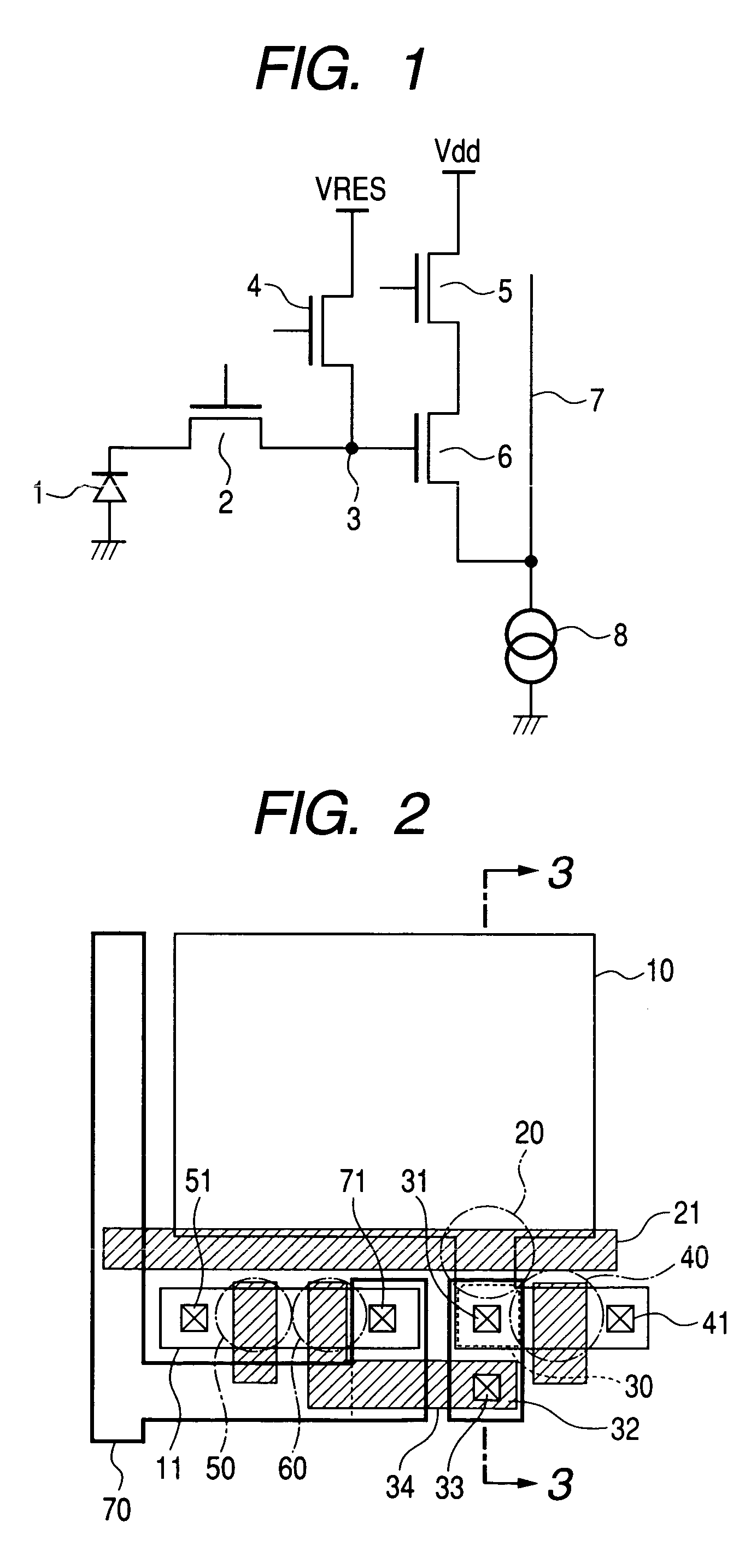
[0050]FIG. 4 shows a layout of a pixel circuit for explaining a first embodiment according to the present invention. Reference numeral 110 denotes an active area in which a photodiode is formed, and 111 denotes an active area in which a selection MOS transistor and a source follower transistor are formed. Reference numeral 120 denotes an area of a transfer MOS transistor and 121 denotes a gate line of the transfer MOS transistor. An area 130 surrounded by a broken line shows a portion formed of a PN junction of semiconductor in the floating diffusion.

[0051] A difference from the prior art form is that leading-out of an electrode from the floating diffusion is effected by a direct contact with a polysilicon 131. The polysilicon 131 serves directly as a gate electrode of a source follower MOS transistor with no intermediary of a metallic electrode. Reference numeral 132 denotes a shading metal covering over the floating diffusion, which shading metal in the present embodiment covers ...

second embodiment

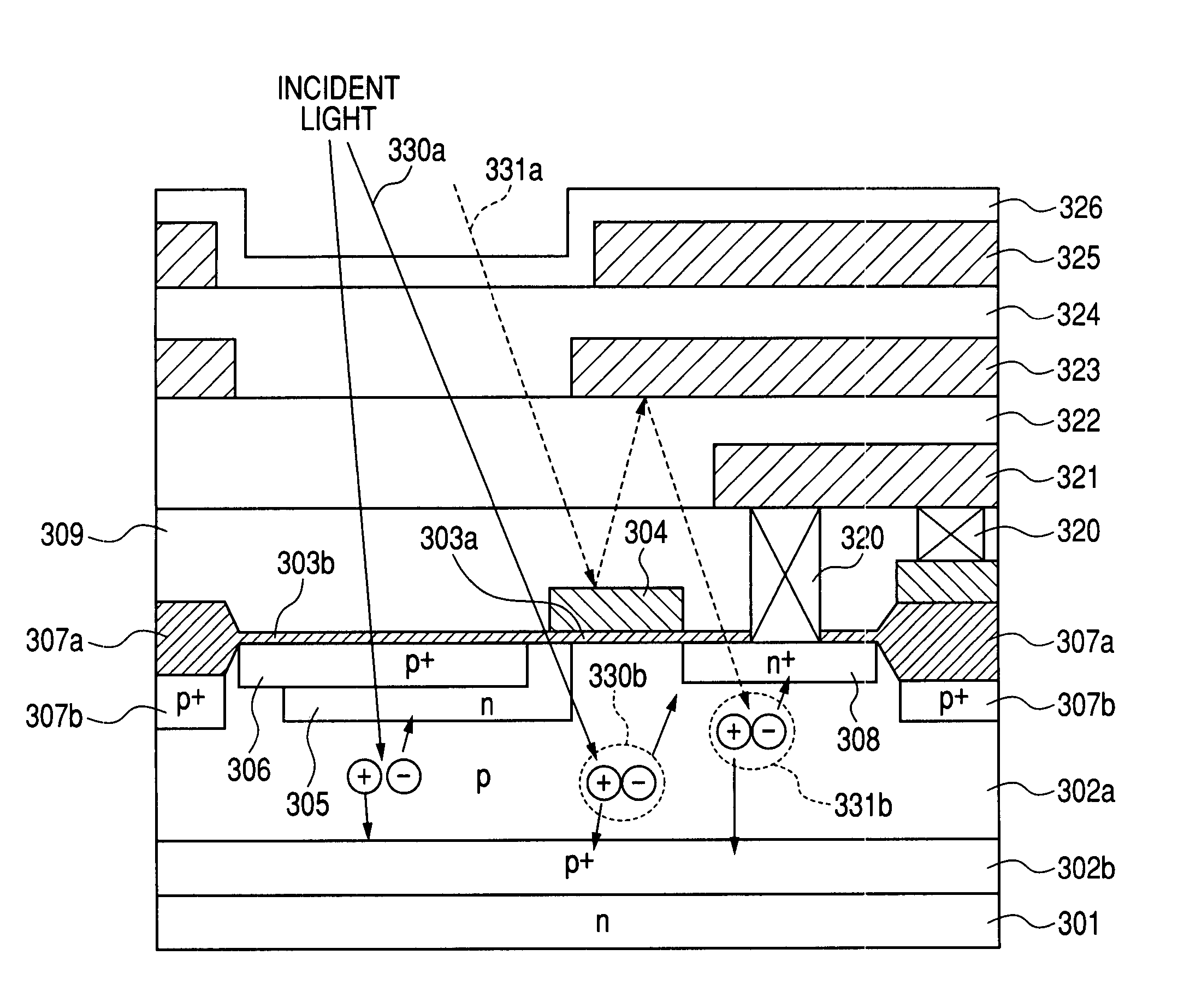
[0062]FIG. 6 is a sectional view of a pixel section of a solid-state image pick-up device of a second embodiment according to the present invention. Reference numeral 601 denotes an n-type silicon substrate, 602a denoting a P-type well, 602b denoting a P-type embedded layer, 603a denoting a gate oxide film of a MOS transistor, 603b denoting a thin oxide film on a light receiving section, 604 denoting a gate electrode of a transfer MOS transistor, 605 denoting an N-type cathode of the photodiode 1, 606 denoting a surface P-type region for making the photodiode formed into an embedded structure, 607a denoting a LOCOS oxide film for element isolation, 607b denoting a P-type channel stop layer, and 608a denoting an N-type high concentration region which forms a floating diffusion and which is also formed to be a drain region of the transfer MOS transistor. Reference character 608b denotes a polysilicon lead-out electrode brought into direct contact with the N-type high concentration reg...

third embodiment

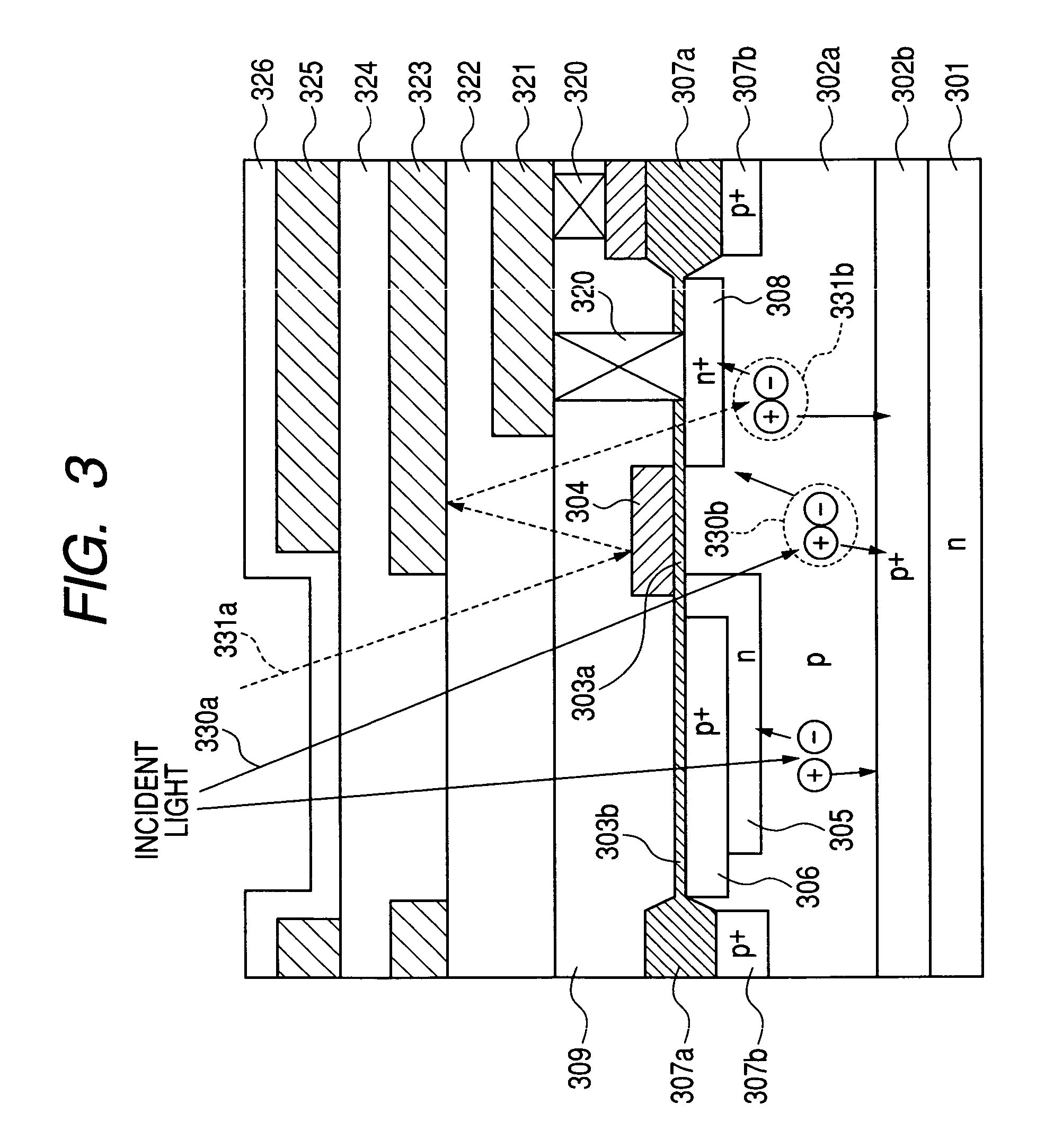
[0064]FIG. 7 is a sectional view of a pixel section of a solid-state image pick-up device of a third embodiment according to the present invention. Reference numeral 701 denotes an N type silicon substrate, 702 denoting a embedded P-type high concentration layer, 703a denoting an N-type epitaxial layer, 703b denoting an N-type cathode of a photodiode, 704a, 704b, 704c denoting P-type isolation layers, and 705a, 705b, 705c denoting P-type well layers. Reference characters 706a, 706b denote channel stop P-type layers below a field oxide film. Reference numeral 714 denotes a field stop layer defining a charge transfer path to a floating diffusion to form a potential barrier directly under a transfer MOS transistor, 707 denoting the field oxide film, 708 denoting a gate oxide film of a MOS transistor, 709a denoting a gate polysilicon of the transfer MOS transistor, on which surface a metal silicide layer 709b is provided and 710 denoting a surface P-type layer for forming the photodiode...


PUM


Abstract

The present invention provides a solid-state image pick-up device without shading in the dark state, and capable of making a dynamic range and a S/N high. Reference numeral 505 denotes an N-type cathode of a photodiode, 506 denoting a surface P-type region for forming the photodiode into an embedded structure, 508a denoting an N-type high concentration region which forms a floating diffusion and which is also a drain region of a transfer MOS transistor. Reference character 508b denotes a polysilicon lead-out electrode brought into direct contact with the N-type high concentration region. Light incident from the surface passes through an aperture without a metal third layer 525 to enter into the photodiode. Among incident lights, light reflected by the top surface of a gate electrode 504 of the transfer MOS transistor is reflected by a first layer metal 521 right above the polysilicon, so as to repeats reflection a plurality of times to attenuate sufficienly before entering into the floating diffusion section, thereby making the aliasing extremely small.

Description

BACKGROUND OF THE INVENTION [0001] 1. Field of the Invention [0002] The present invention relates to a solid-state image pick-up device used for a digital camera, etc., as an image pick-up device for inputting a picture. [0003] 2. Related Background Art [0004] In recent years, there has been a rapidly increasing demand on a solid-state image pick-up device used mainly for a digital still camera and a video camcorder, as an image pick-up device for inputting a picture. [0005] As such solid-state image pick-up device, CCD (Charge Coupled Device) and MOS type sensors are used. Although the former, which has a high sensitivity and a low noise level in comparison with the latter, has been widely used as an image pick-up device of high picture quality, the former has disadvantages such as a large power consumption, a high drive voltage, a high cost due to the fact that the ordinary semiconductor manufacturing process cannot be applied, and a difficulty in integrating peripheral circuits s...

Claims


Application Information

Patent Timeline
IPC IPC(8): H01L27/146H04N5/335H04N5/355H04N5/361H04N5/369H04N5/374
CPCH01L21/28525H01L23/53271H01L27/14601H01L27/14623H01L27/14612H01L27/14636H01L2924/0002H01L27/1463H01L2924/00
Inventor INOUE, SHUNSUKE
Owner CANON KK
Why Eureka
Try Eureka