UV nanoimprint lithography process and apparatus

a lithography and nano-imprint technology, applied in the field of uv nano-imprint lithography process and its apparatus, can solve the problems of high pressure (about 30 atmospheric pressure) required to imprint high-viscosity resists, breakage or damage previously fabricated nanostructures, and opaque stamps used in these processes are also an obstacle to multi-layer alignment, so as to achieve efficient forming of high-precision, high-quality nanostructures

Active Publication Date: 2005-08-25
KOREA INST OF MASCH & MATERIALS
View PDF6 Cites 87 Cited by
  • Summary
  • Abstract
  • Description
  • Claims
  • Application Information

AI Technical Summary

Benefits of technology

[0014] The present invention provides a UV nanoimprint lithography process and its apparatus capable of eff

Problems solved by technology

This makes them inapplicable to the implementation of semiconductor devices, a multi-layer process, because thermal deformation occurring in these technologies will hinder multi-layer alignment.
Furthermore, high pressure (about 30 atmospheric pressures) required to imprint high-viscosity resist can break or damage previously fabricated nanostructures.
Opaque stamps used in these processes are also an obstacle to the multi-layer alignment.
However, the gap distribution between the stamp and the wafer for use in the UV nanoimprint lithography process is not constant (e.g., Si wafer: 20˜30 μm), so that

Method used


Image

  • UV nanoimprint lithography process and apparatus
  • UV nanoimprint lithography process and apparatus
  • UV nanoimprint lithography process and apparatus

Examples


Embodiment Construction

[0038] Now, embodiments of the present invention will be described with reference to the attached drawings.

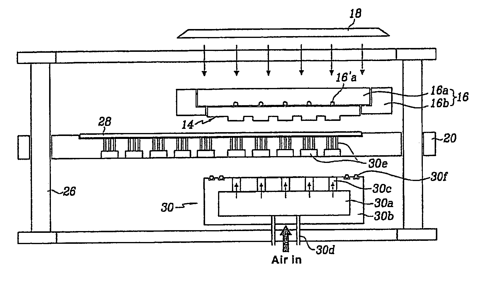
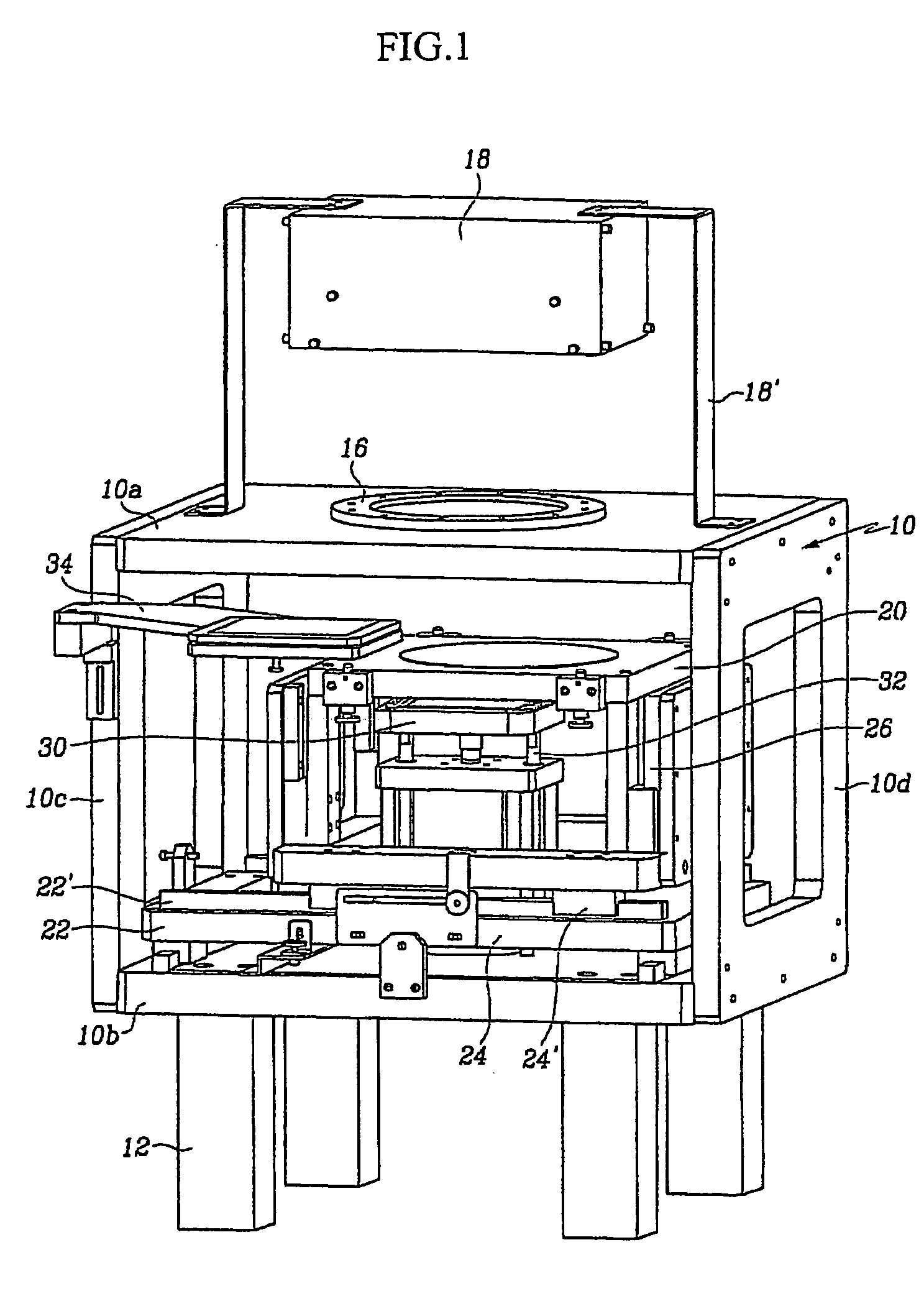
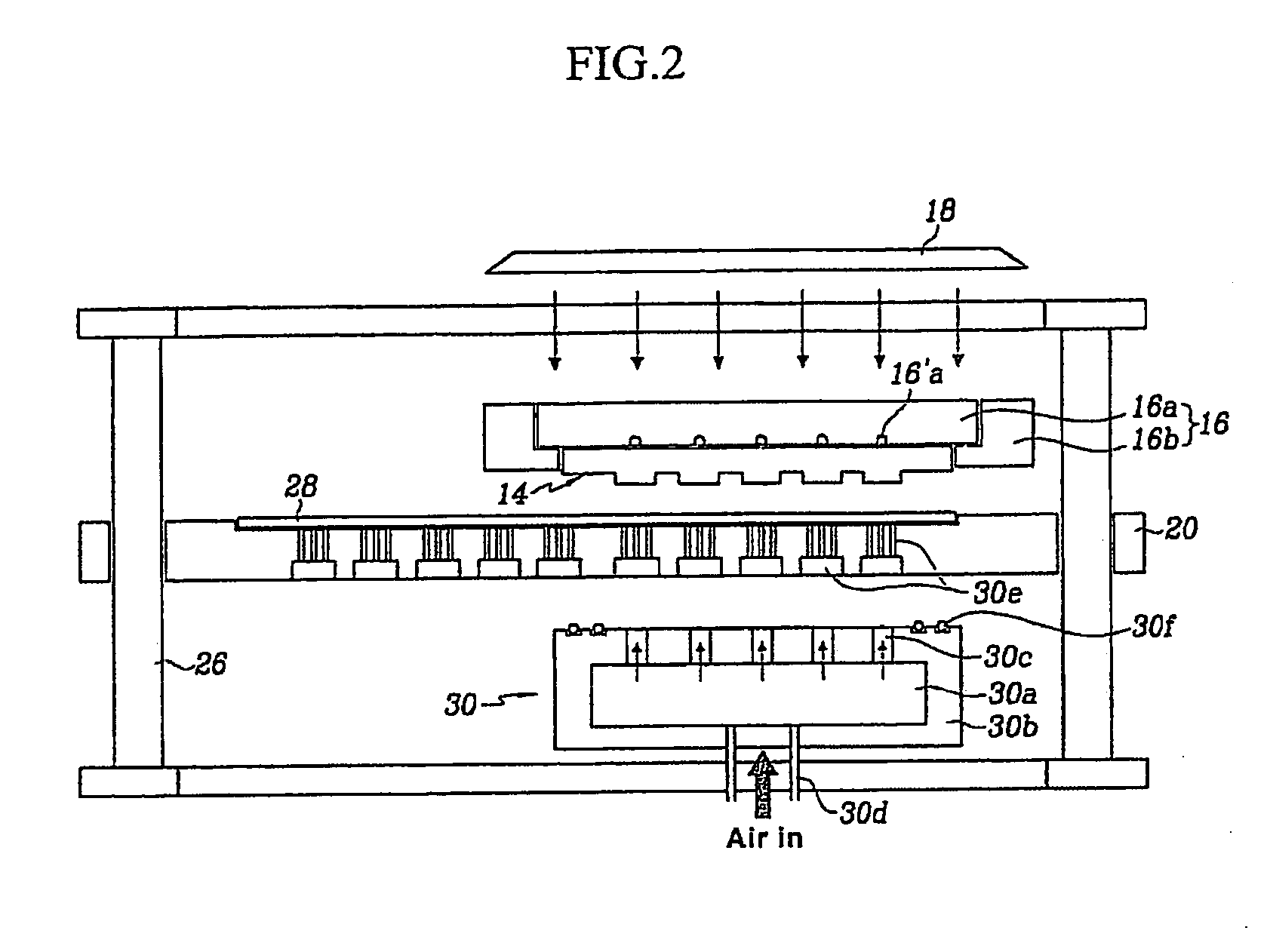
[0039]FIG. 1 is a schematic perspective view showing a UV nanoimprint lithography apparatus according to an embodiment of the present invention, and FIG. 2 is a side view for the UV nanoimprint lithography apparatus of FIG. 1.

[0040]FIG. 1 depicts the apparatus including a base 10 having upper and lower frames 10a and 10b and left and right frames 10c and 10d. The base 10 is supported by four supporting corners 12 arranged on the lower plate 10b.

[0041] As shown in FIG. 2, a stamp chuck 16 mounting an element-wise patterned stamp 14 is fixedly arranged on the upper frame 10a. The stamp chuck 16 is made of a UV-transparent material and includes a back plate 16a for vacuum absorption of the element-wise patterned stamp 14 and the main body 16b mounting the back plate 16a, as shown in FIG. 2.

[0042] Although not shown in detail, the back plate 16a includes a vacuum line 16′a for ...


PUM

PropertyMeasurementUnit
Pressureaaaaaaaaaa
Heightaaaaaaaaaa
Transparencyaaaaaaaaaa

Abstract

A UV nanoimprint lithography process and its apparatus that are able to repeatedly fabricates nanostructures on a substrate (wafer, UV-transparent plate) by using a stamp that is as large as or smaller than the substrate in size are provided. The apparatus includes a substrate chuck for mounting the substrate; a stamp made of UV-transparent materials and having more than two element stamps, wherein nanostructures are formed on the surface of each element stamp; a stamp chuck for mounting the stamp; a UV lamp unit for providing UV light to cure resist applied between the element stamps and the substrate; a moving unit for moving the substrate chuck or the stamp chuck to press the resist with the element stamps and substrate; and a pressure supply unit for applying pressurized gas to some selected regions of the substrate to help complete some incompletely filled element stamps.

Description

CROSS REFERENCE TO RELATED APPLICATION [0001] This application claims priority to and the benefit of Korean Patent Application No. 10-2004-0012191, filed on Feb. 24, 2004, which is hereby incorporated by reference for all purposes as if fully set forth herein BACKGROUND OF THE INVENTION [0002] (a) Field of the Invention [0003] The present invention relates to a UV nanoimprint lithography process and its apparatus, and more specifically, to a UV nanoimprint lithography process and its apparatus capable of repeatedly fabricating nanostructures on a substrate (e.g. wafer, glass, quartz, etc.) with a stamp having the nanostructures engraved thereon. [0004] (b) Description of Related Art [0005] The UV nanoimprint lithography technology is an economical and effective method of fabricating nanostructures It is multidisciplinary, so that it should be supported by various technologies from such fields as nano-scale materials science, stamp fabrication, ant-adhesion layer, etching and measure...

Claims


Application Information

Patent Timeline
IPC IPC(8): B29C35/08G03F7/20B29C59/02G03F7/00
CPCB29C35/0888B29C59/022B29C2035/0827G03F7/0002B82Y10/00B82Y30/00B82Y40/00B29C2059/023Y10S977/887A41C3/10A41C3/142
Inventor JEONG, JUN-HOSOHN, HYONKEESIM, YONG-SUKSHIN, YOUNG-JAELEE, EUNG-SUGWHANG, KYUNG-HYUN
Owner KOREA INST OF MASCH & MATERIALS
Why Eureka
Try Eureka