Wafer probe station having a skirting component

a probe station and component technology, applied in the field of probe stations, can solve the problems of time-consuming and laborious custom set-up of such probe stations required for guarding and kelvin connection procedures, significant time-consuming alteration of such stations, and limited effectiveness, so as to reduce settling time, reduce energy transfer, and increase sensitivity

Inactive Publication Date: 2005-08-25
CASCADE MICROTECH
View PDF99 Cites 5 Cited by
  • Summary
  • Abstract
  • Description
  • Claims
  • Application Information

AI Technical Summary

Benefits of technology

[0020] The signal line guarding system just described can thus be energized via the connector mechanism so that virtually no potential difference is developed between the signal line element and its surrounding guard enclosure. Hence, the level of leakage current flowing away from the signal line element is reduced to virtually zero which enables low-level currents in the system to be measured with increased sensitivity. Also, since there is a reduction in the combined area of the conductive surfaces to which the signal line element is capacitively coupled, less energy transfer and time is required for this line element to acquire its full potential, so that settling-time is reduced. Moreover, if any transient shifts in electrical state should occur in relation to any nonconductor or conductor located outside the guard enclosure, this will have virtually no effect on the signal line element due to the effective barrier against radiation provided by the conductive guard enclosure, so that measurement instability is reduced.

Problems solved by technology

However the custom set-up of such probe stations required for guarding and Kelvin connection procedures is time-consuming and, in some instances, limited as to effectiveness.
Accordingly significant time-consuming alteration of such a station would be required to obtain both a guarded and shielded chuck assembly.
The probes on the probe card, on the other hand, are both guarded and shielded; however there is no means of enabling each probe to be moved independently of the others in unison with its guard and shield to accommodate different contact patterns of test devices, thus sacrificing flexibility of the probe station.
However such wiring requires time-consuming set-up, particularly if Kelvin connections are also required.
Moreover, the use of sheet insulation to insulate the copper guarding layer, from the add-on surface and the underlying chuck assembly fails to provide as low a dielectric constant between the respective elements as is desirable to minimize leakage currents in view of the low level of current to be measured.
With respect to -probe stations that are designed to accommodate the measurement of low levels of current, a sensitivity threshold is normally encountered below which further improvements in current sensitivity are difficult to reliably achieve.
A particular difficulty encountered in low-level current measurements is the excessive time required for measurement voltages to stabilize with reference to the device under test after a shift in voltage has occurred at the electrical input to the probe station.
This problem of excessive settling time, as it is referred to, increases as the level of current under measurement is reduced.
That is, due to the residual capacitance existing between spaced apart conductors in the region surrounding the immediate test site, a certain amount of time is required for the conductors that are in direct connection with the test device to fully charge or discharge to their desired voltages, and the time required will increase as the current through the device decreases.
In addition to settling effects, measurements of low level currents are also susceptible to error due to electrical discharge effects which occur because of the acceptance and release of charge by nonconductors in the region surrounding the immediate test site.
At very low currents, these discharge effects can significantly-distort measurement values and hence contribute to unacceptable levels of measurement instability.

Method used


Image

  • Wafer probe station having a skirting component
  • Wafer probe station having a skirting component
  • Wafer probe station having a skirting component

Examples


Embodiment Construction

General Arrangement of Probe Station

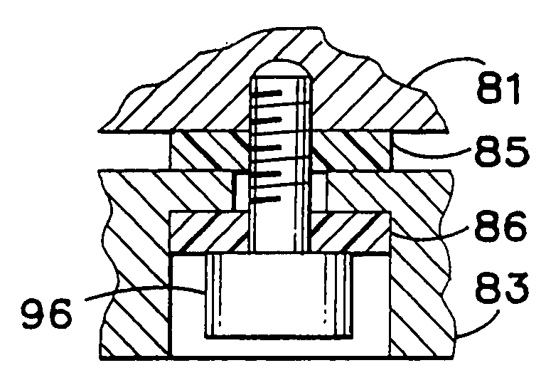
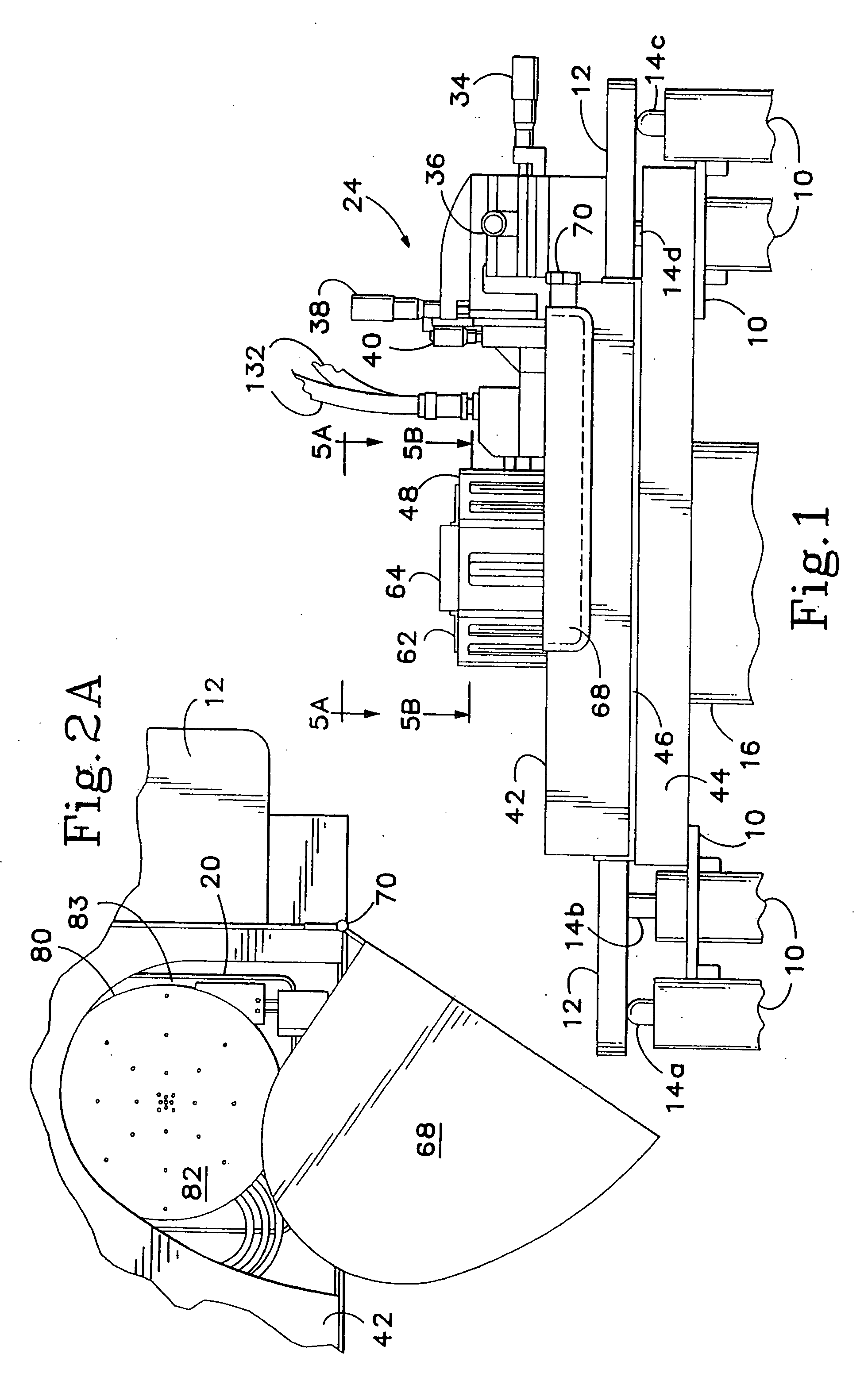
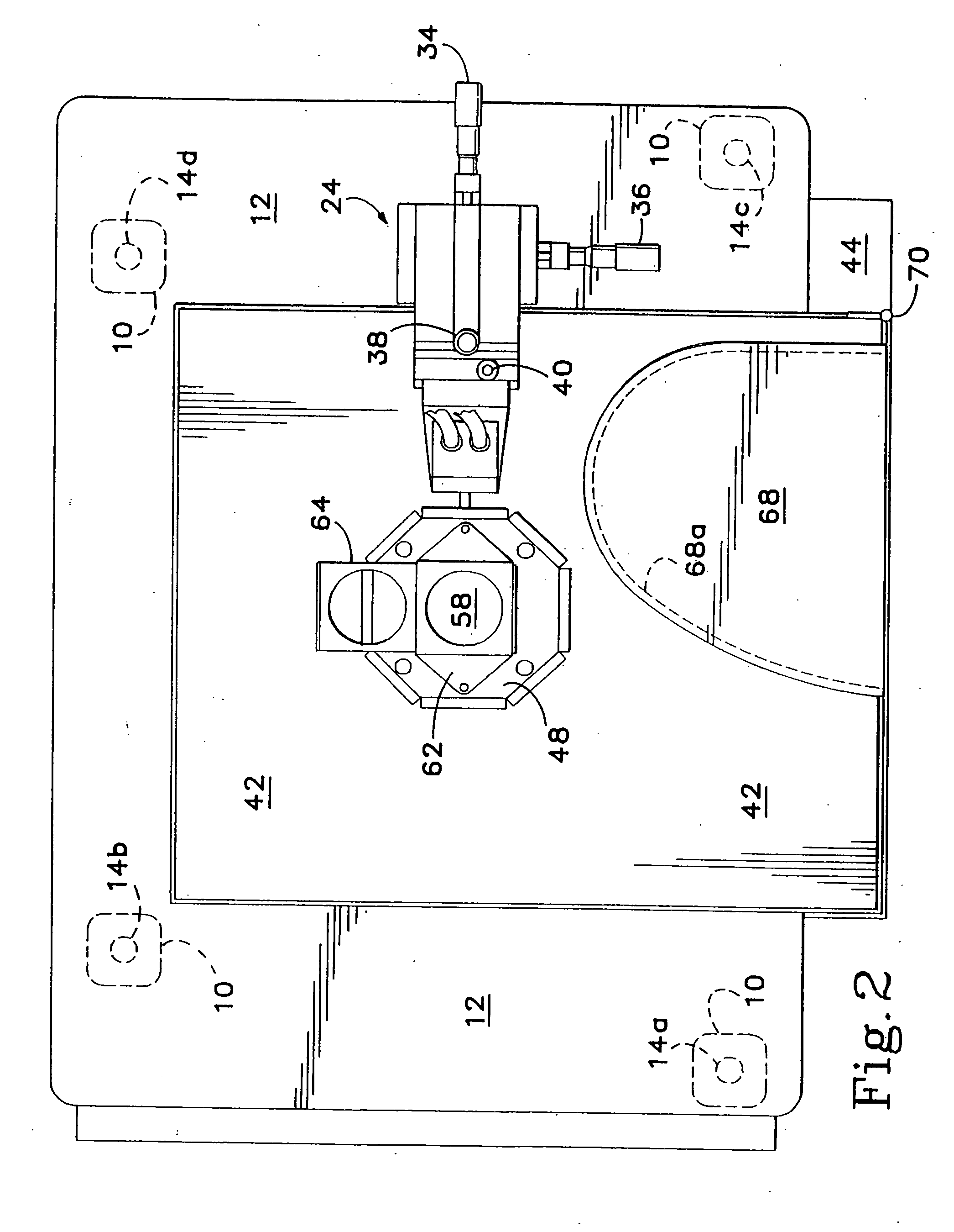
[0041] With reference to FIGS. 1, 2 and 3, an exemplary embodiment of the probe station of the present invention comprises a base 10 (shown partially) which supports a platen 12 through a number of jacks 14a, 14b, 14c, 14d which selectively raise and lower the platen vertically relative to the base by a small increment (approximately one-tenth of an inch) for purposes to be described hereafter. Also supported by the base 10 of the probe station is a motorized positioner 16 having a rectangular plunger 18 which supports a movable chuck assembly 20 for supporting a wafer or other test device. The chuck assembly 20 passes freely through a large aperture 22 in the platen 12 which permits the chuck assembly to be moved independently of the platen by the positioner 16 along X, Y and Z axes, i.e. horizontally along two mutually-perpendicular axes X and Y, and vertically along the Z axis. Likewise, the platen 12, when moved vertically by the jacks 14, mo...


PUM


Abstract

A probe station includes a fully guarded chuck assembly and connector mechanism for increasing sensitivity to low-level currents while reducing settling times. The chuck assembly includes a wafer-supporting first chuck element surrounded by a second chuck element having a lower component, skirting component and upper component each with a surface portion extending opposite the first element for guarding thereof. The connector mechanism is so connected to the second chuck element as to enable, during low-level current measurements, the potential on each component to follow that on the first chuck element as measured relative to an outer shielding enclosure surrounding each element. Leakage current from the first chuck element is thus reduced to virtually zero, hence enabling increased current sensitivity, and the reduced capacitance thus provided by the second chuck element decreases charging periods, hence reducing settling times. With similar operation and effect, where any signal line element of the connector mechanism is arranged exterior of its corresponding guard line element, such as adjacent the chuck assembly or on the probe-holding assembly, a guard enclosure is provided to surround and fully guard such signal line element in interposed relationship between that element and the outer shielding enclosure.

Description

[0001] This is a continuation of U.S. patent application Ser. No. 08 / 100,494 filed on Aug. 2, 1993, which, in turn, is a continuation-in-part of U.S. patent application Ser. No. 07 / 896,853 filed on Jun. 11, 1992, now U.S. Pat. No. 5,345,170.BACKGROUND OF THE INVENTION [0002] The present invention is directed to probe stations adapted for making highly accurate low-current and low-voltage measurements of wafers and other electronic test devices. More particularly, the invention relates to such a probe station having a guarding system for preventing current leakage, a Kelvin connection system to eliminate voltage losses caused by line resistances, and an electromagnetic interference (EMI) shielding system. [0003] The technique of guarding to minimize current leakage during low-current measurements, the use of Kelvin connections for low-voltage measurements, and the provision of EMI shielding are all well known and discussed extensively in the technical literature. See, for example, an...

Claims


Application Information

Patent Timeline
Patent Type & Authority Applications(United States)
IPC IPC(8): H01L21/66A46D1/00G01R1/067G01R1/073G01R31/02G01R31/28H01L21/687
CPCA46D1/00G01R1/0416G01R1/06705G01R1/06794H01L21/68785G01R1/18G01R31/2886G01R31/2887G01R1/07392
Inventor SCHWINDT, RANDY J.HARWOOD, WARREN K.TERVO, PAUL A.SMITH, KENNETH R.WARNER, RICHARD H.
Owner CASCADE MICROTECH
Why Eureka
Try Eureka