Method for manufacturing conductive element substrate, conductive element substrate, method for manufacturing liquid crystal display, liquid crystal display and electronic information equipment

a technology of conductive elements and substrates, applied in the direction of identification means, instruments, static indicating devices, etc., can solve the problems of affecting the display quality, and bringing about electrolytic corrosion, so as to achieve the effect of high film strength, and reducing the etch ra

Inactive Publication Date: 2005-08-25
SHARP KK
View PDF25 Cites 33 Cited by
  • Summary
  • Abstract
  • Description
  • Claims
  • Application Information

AI Technical Summary

Benefits of technology

[0101] If the conductive element constituted of a plurality of layers is formed to have the upward-tapered cross section as shown in FIG. 22, high film strength is given to the lower layer even if the thus obtained conductive element is a finally obtained one or further subjected to any other manufacturing steps. Thus, the lower layer is prevented from coming off.
[0102] According to the method for manufacturing the conductive element substrate of the present invention, a conductive element is formed by patterning the laminated conductive film which is constituted of the first conductive metal film and the second conductive metal film which is formed on the first conductive metal film and is lower in etch rate than the first conductive metal film. The method includes the second etching step for etching the second conductive metal film only. Therefore, in the first etching step in which the first and second conductive metal films are etched simultaneously, the edge portions of the second conductive metal film may remain protruding more outward than the edge portions of the underlying film due to the difference in etch rate between the first and second conductive metal films for forming the laminated conductive film. However, the protruding edge portions of the second conductive metal film are etched away in the second etching step. Therefore, eventually, the edge portions of the second conductive metal film will not remain protruding. Thus, in the manufacture of the conductive element by patterning the first conductive metal film and the second conductive metal film which is lower in etch rate than the first conductive metal film in the course of manufacture of the conductive element substrate, a decrease in manufacturing yield due to coming off of the edge portions of the second conductive metal fiim is prevented.

Problems solved by technology

In this case, the transparent and reflecting electrodes show different electrode potentials, which possibly leads to defective display.
However, if the voltage applied to the liquid crystal layer is distorted by parasitic capacitance of TFTs or the like, a direct voltage may possibly be applied to the liquid crystal layer.
In such a case, a direct voltage is applied to the liquid crystal layer to cause variations in light intensity (flicker), resulting in significant decrease in display quality.
The reason why the ITO film is not formed on the aluminum film is that the aluminum film and the ITO film bring about electrolytic corrosion when they come into to contact in the course of electrode formation and the ITO film is dropped off.
Thus, the IZO layer is reduced in strength and likely to come off.
In this case, a short circuit occurs between the pixel electrodes to decrease a manufacturing yield of the active matrix substrate.

Method used


Image

  • Method for manufacturing conductive element substrate, conductive element substrate, method for manufacturing liquid crystal display, liquid crystal display and electronic information equipment
  • Method for manufacturing conductive element substrate, conductive element substrate, method for manufacturing liquid crystal display, liquid crystal display and electronic information equipment
  • Method for manufacturing conductive element substrate, conductive element substrate, method for manufacturing liquid crystal display, liquid crystal display and electronic information equipment

Examples


embodiment 1

[0156] Hereinafter, a liquid crystal display of Embodiment 1 of the present invention will be described.

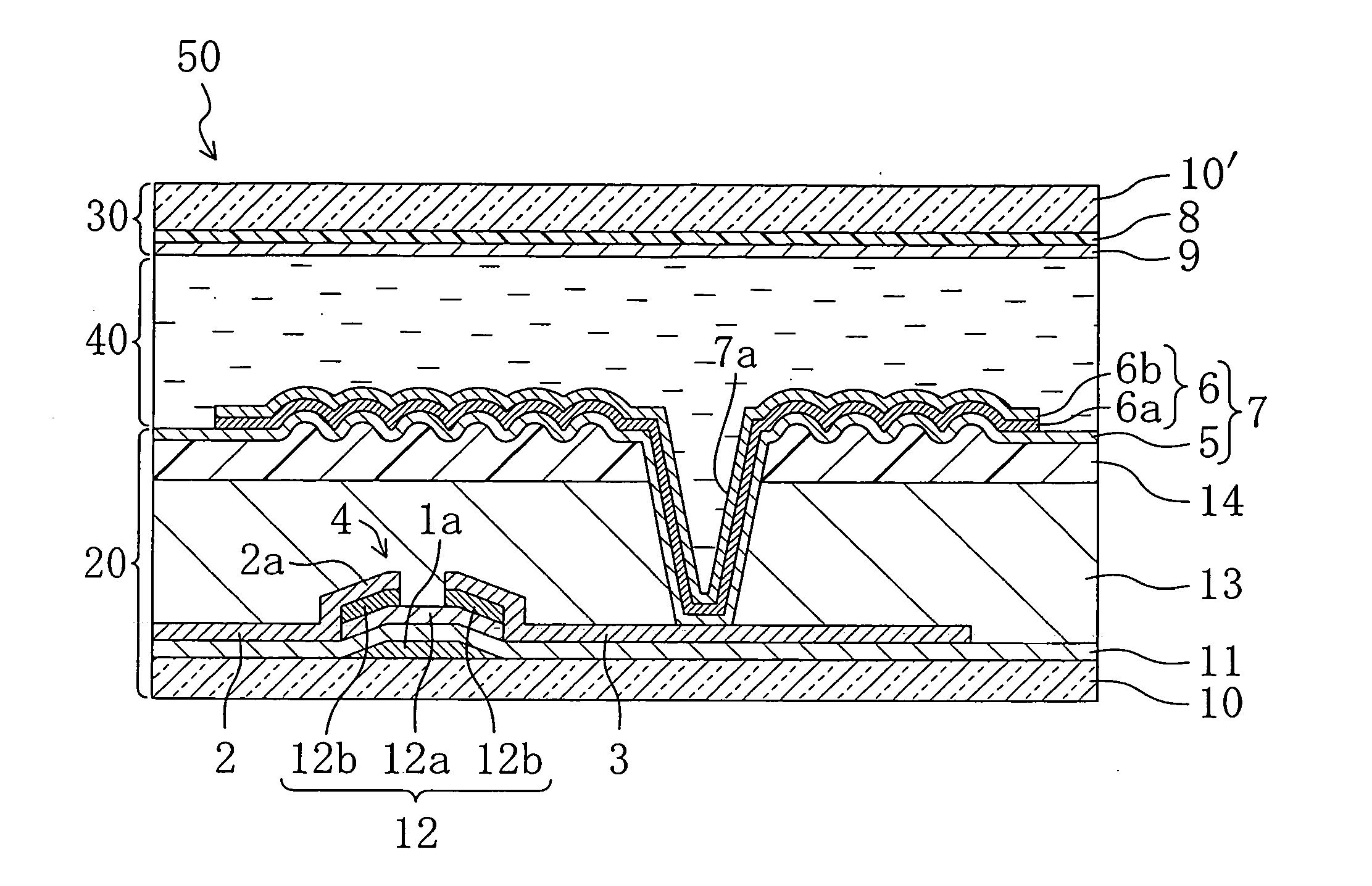
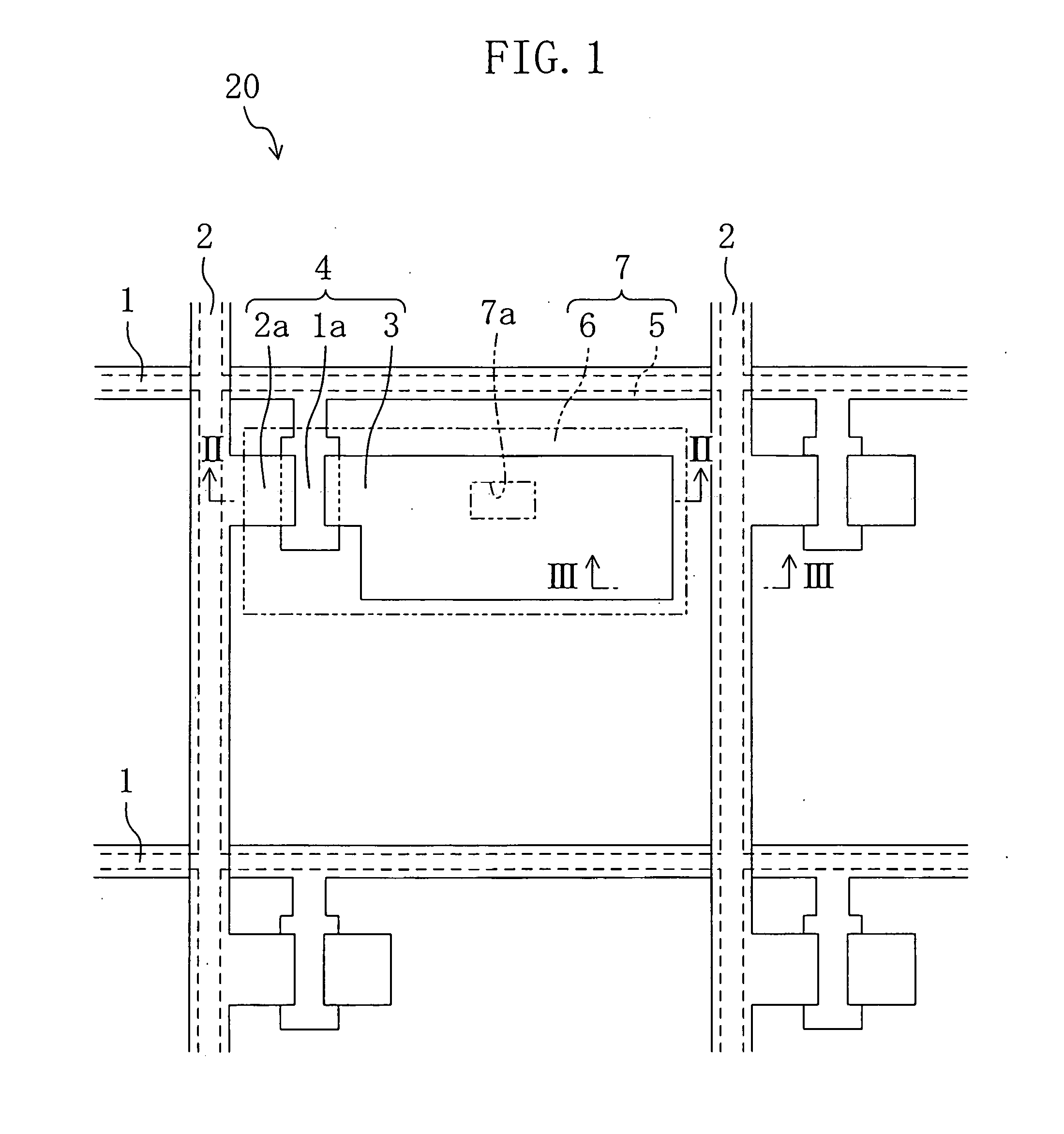
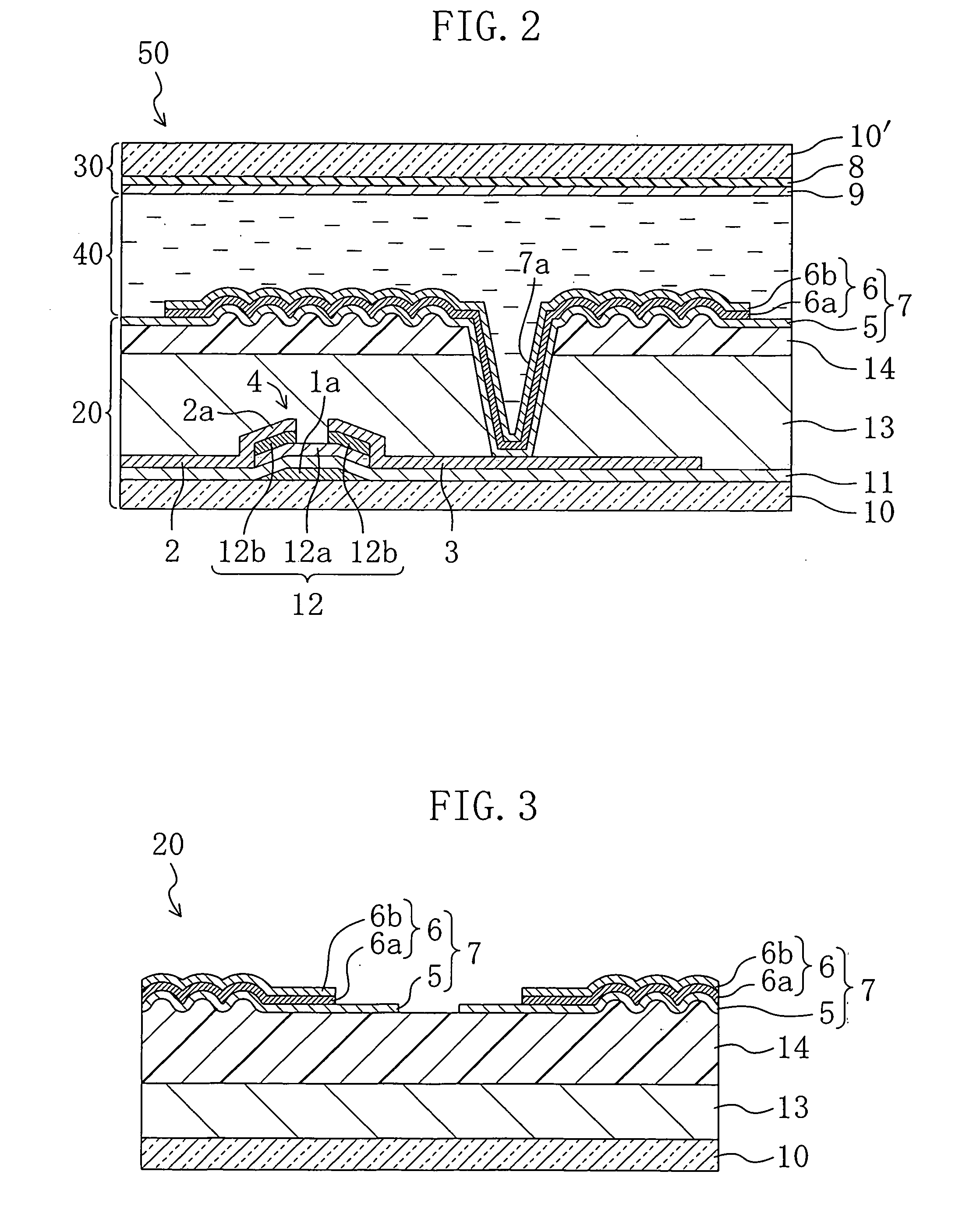
[0157]FIG. 1 is a schematic plan view of an active matrix substrate 20 for forming a liquid crystal display 50 according to Embodiment 1 of the present invention. FIG. 2 is a schematic sectional view of the liquid crystal display 50 cut along the line II-II shown in FIG. 1. FIG. 3 is a schematic sectional view of the active matrix substrate 20 cut along the line III-III shown in FIG. 1, illustrating a section of the edge portions of two adjacent pixels.

[0158] The liquid crystal display 50 includes the active matrix substrate 20, a counter substrate 30 opposed to the active matrix substrate 20 and a liquid crystal layer 40 sandwiched between the substrates 20 and 30.

[0159] As to the active matrix substrate 20, a plurality of gate lines 1 extending parallel to each other and a plurality of source lines 2 extending parallel to each other are arranged on a glass substrate 10 and th...

embodiment 2

[0218] A liquid crystal display according to Embodiment 2 of the present invention will be described below.

[0219] The liquid crystal display according to Embodiment 2 and an active matrix substrate for manufacturing the liquid crystal display are substantially the same in plane structure and sectional structure as those described in Embodiment 1 except the manufacturing method thereof. Therefore, in the following embodiment, explanation is given principally of a method of manufacturing the liquid crystal display, in particular, the step of manufacturing the active matrix substrate.

[Step of Manufacturing Active Matrix Substrate]

[0220] Hereinafter, explanation is given of the step of manufacturing an active matrix substrate according to Embodiment 2 of the present invention with reference to the drawings. The step includes a TFT formation step, a laminated conductive film formation step and a reflecting electrode formation step. FIGS. 11 to 13 are schematic sectional views correspo...

embodiment 3

[0261]FIG. 22 is a sectional view of a major part illustrating a schematic configuration of an electrode wiring substrate (conductive element substrate) according to Embodiment 3.

[0262] As shown in FIG. 22, the electrode wiring substrate 107 includes a glass substrate 101 provided with an IZO layer (second conductive metal layer) 104 which is formed as an uppermost layer having a lower etch rate and an aluminum (Al) layer (first conductive metal layer) 103 and a molybdenum (Mo) layer (first conductive metal layer) 102 which are formed as a lower layer having a higher etch rate. When viewed in cross section, the uppermost IZO layer (second conductive metal layer) 104 is more narrowed in the horizontal direction than the underlying Al layer (first conductive metal layer) 103 and Mo layer (first conductive metal layer) 102. The thus obtained layered structure has a cross section which is substantially tapered upward from the closest layer to the substrate, thereby providing a layered ...


PUM

PropertyMeasurementUnit
thicknessaaaaaaaaaa
light energyaaaaaaaaaa
thicknessaaaaaaaaaa

Abstract

A method for manufacturing a liquid crystal display which employs an active matrix substrate including a plurality of pixels arranged in matrix on a substrate and reflecting electrodes formed in the pixels, respectively. The method comprises (a) a laminated conductive film formation step of sequentially forming a conductive metal film and an amorphous transparent conductive film on a substrate to form a laminated conductive film and (b) a reflecting electrode formation step of patterning the laminated conductive film into a reflecting electrode, wherein the step (b) includes a first etching step of etching the conductive metal film and the amorphous transparent conductive film simultaneously and a second etching step of etching the amorphous transparent conductive film only.

Description

CROSS-REFERENCE TO RELATED APPLICATIONS [0001] This non-provisional application claims priority under 35 U.S.C. §119(a) on Japanese Patent Applications Nos. 2004-43711 filed on Feb. 19, 2004, 2004-96823 filed on Mar. 29, 2004 and 2005-xxxxx filed on xxxxx, 2005, the entire contents of which are hereby incorporated by reference. BACKGROUND OF THE INVENTION [0002] (a) Field of the Invention [0003] The present invention relates to a method for manufacturing a conductive element substrate. In particular, it relates to a method for manufacturing reflecting electrodes on an active matrix substrate for forming a liquid crystal display. [0004] (b) Description of Related Art [0005] Semi-transmissive liquid crystal displays, which are one of liquid crystal displays, are capable of displaying in both transmissive and reflective modes. The semi-transmissive liquid crystal displays are given with a feature of a transmissive liquid crystal display such as high visibility in dark place owing to a ...

Claims


Application Information

Patent Timeline
Patent Type & Authority Applications(United States)
IPC IPC(8): C09K19/00C23F1/00C23F1/02C23F1/16C23F1/20C23F1/26C23F1/44G02F1/133G02F1/1335G02F1/1343G02F1/1362G09F9/00G09F9/30
CPCC23F1/02C23F1/16C23F1/20C23F1/26C23F1/44G02F1/133553Y10S438/978G02F1/13439G02F1/136227Y10T428/1064Y10T428/1055Y10T428/10G02F1/133555C09K2323/00C09K2323/04C09K2323/051H02G7/02H02G7/053
Inventor ISHIZUKA, KAZUHIROFUJIKAWA, TAKASHISAKAI, TAKEHIKO
Owner SHARP KK
Why Eureka
Try Eureka