Electroplating apparatus

Inactive Publication Date: 2005-09-01
TAIWAN SEMICON MFG CO LTD
View PDF5 Cites 23 Cited by
  • Summary
  • Abstract
  • Description
  • Claims
  • Application Information

AI Technical Summary

Benefits of technology

[0023] The electrically-conductive shield may be connected to a shield current source. A switch may be provided between the shield current source and the shield. The switch may be manipulated to apply a negative charge to the shield, in which case the shield acts as a cathode and reduces the quantity of metal cations in the electrolytic fluid in the area adjacent to the edge region as compared to the area adjacent to the center region of the wafer. Consequently, the electroplating metal deposition rate at the edge region is reduced to compensate for the normally lower metal deposition rate at the center region of the wafer, thus enhancing the overall thickness uniformity of the electroplated metal.
[0024] Th

Problems solved by technology

Due to the ever-decreasing size of semiconductor components and the ever-increasing density of integrated circuits on a wafer, the complexity of interconnecting the components in the circuits requires that the fabrication processes used to define the metal conductor line interconnect patterns be subj

Method used


Image

  • Electroplating apparatus
  • Electroplating apparatus
  • Electroplating apparatus

Examples


Example

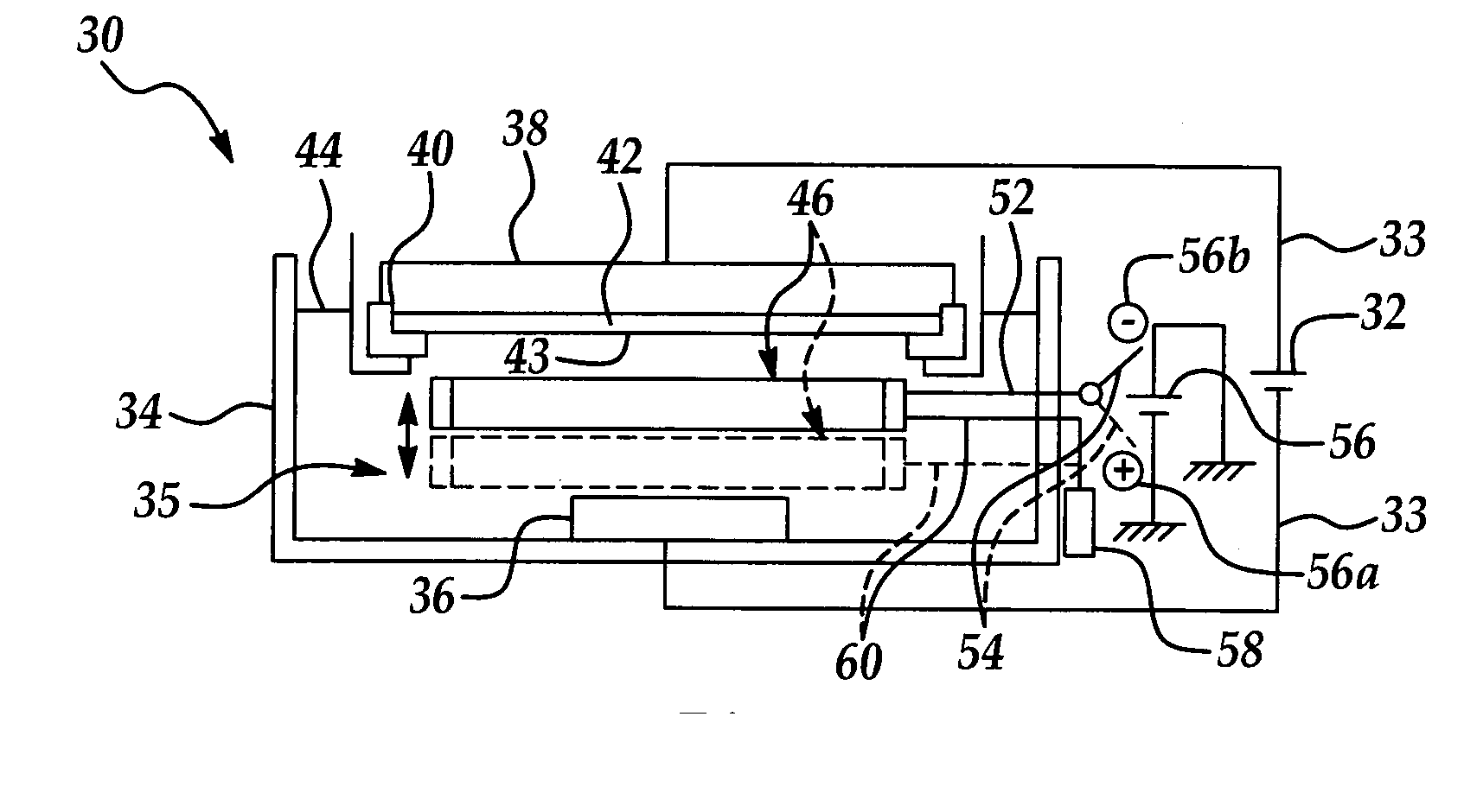
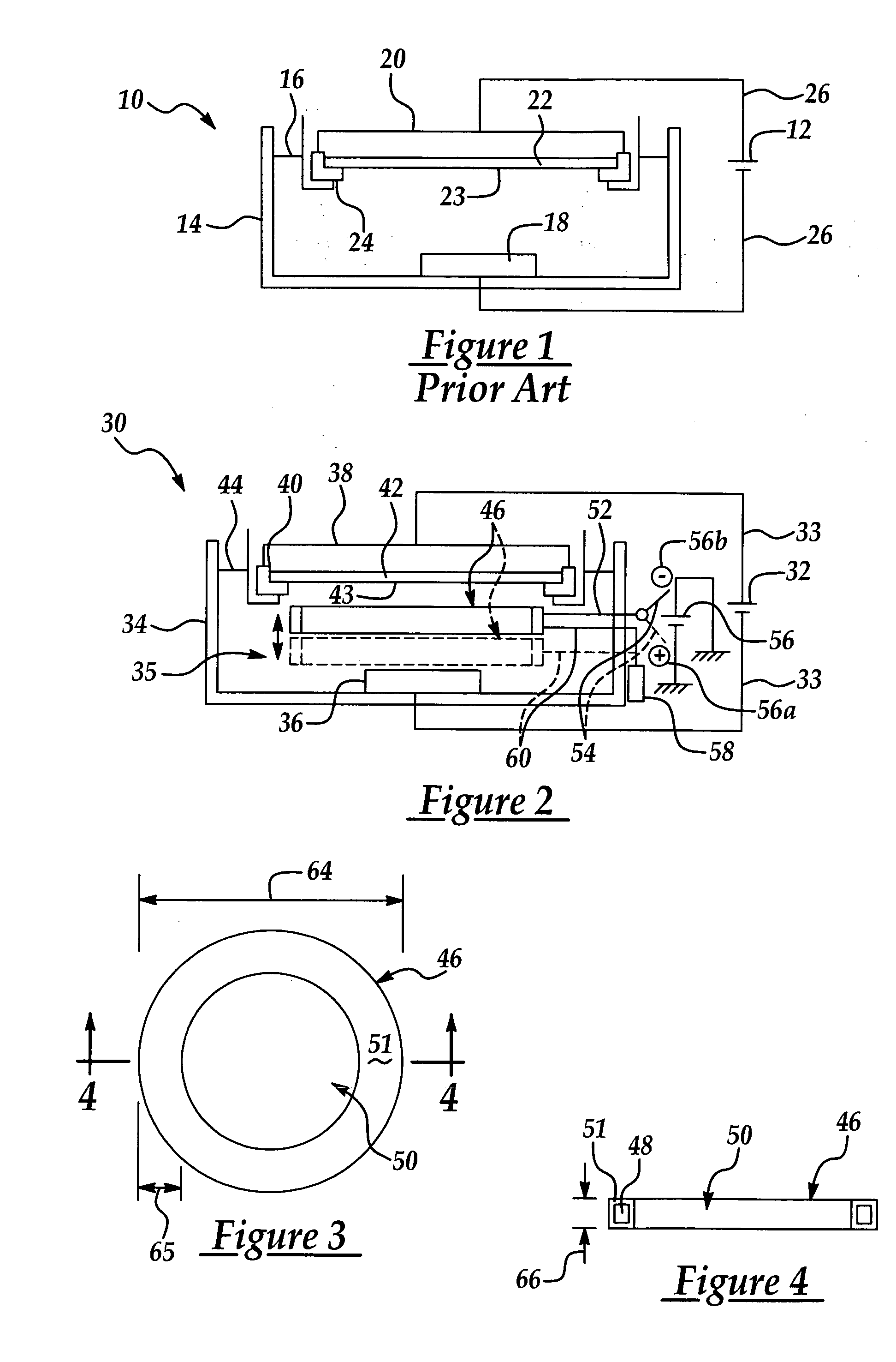
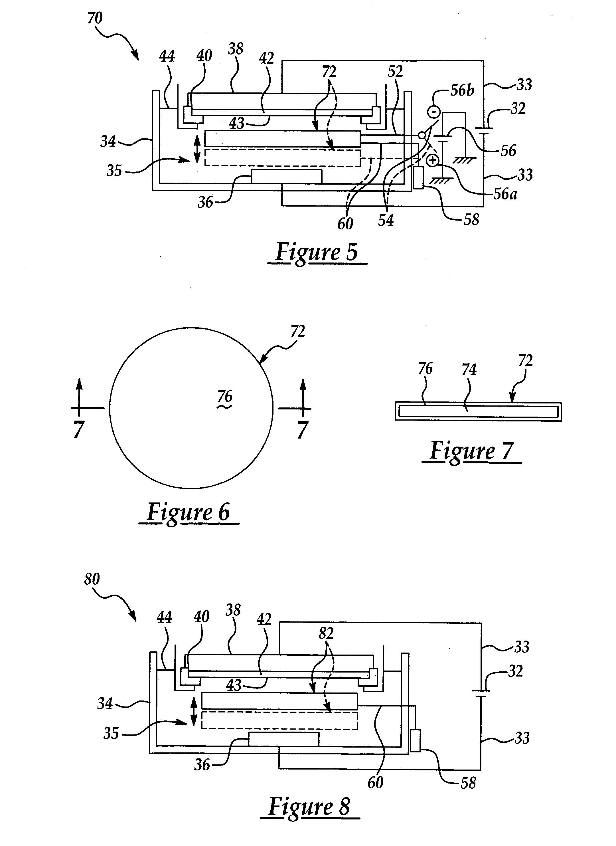
[0034] The present invention has particularly beneficial utility in the electrochemical plating of copper or other metal onto a semiconductor wafer substrate in the fabrication of semiconductor integrated circuits. However, the invention is more generally applicable to the electrochemical plating of metals including but not limited to copper on substrates in a variety of industrial applications, including but not limited to semiconductor fabrication.

[0035] The present invention is generally directed to a novel electroplating apparatus which enhances uniformity in the thickness of a metal layer deposited on a semiconductor wafer. The apparatus facilitates the electroplating of a metal layer having substantially uniform thickness across the entire wafer surface, particularly between the center and edge regions of the wafer. The apparatus includes a bath container having a reservoir for containing an electrolytic fluid. A cathode and an anode immersed in the electrolytic fluid are con...


PUM

PropertyMeasurementUnit
Thicknessaaaaaaaaaa
Electric chargeaaaaaaaaaa
Currentaaaaaaaaaa

Abstract

A electroplating apparatus which is suitable for depositing a metal layer of substantially uniform thickness across the center and edge regions of a semiconductor wafer substrate is disclosed. The apparatus includes a reservoir for containing an electrolytic fluid. A cathode, to which is mounted a wafer, and an anode in the electrolytic fluid are connected to an electroplating current source. A shield is provided between the cathode and anode to facilitate a more uniform deposit of the metal onto the wafer across the entire surface, including the center and edge regions, of the wafer.

Description

FIELD OF THE INVENTION [0001] The present invention relates to electrochemical plating (ECP) apparatuses and processes used to deposit metal layers on semiconductor wafer substrates in the fabrication of semiconductor integrated circuits. More particularly, the present invention relates to an elecroplating apparatus which includes a shield interposed between an anode and a cathode to reduce the electroplating deposition rate at the edge region of a substrate and facilitate deposition of a metal film having a substantially uniform thickness across the entire surface of a wafer. BACKGROUND OF THE INVENTION [0002] In the fabrication of semiconductor integrated circuits, metal conductor lines are used to interconnect the multiple components in device circuits on a semiconductor wafer. A general process used in the deposition of metal conductor line patterns on semiconductor wafers includes deposition of a conducting layer on the silicon wafer substrate; formation of a photoresist or oth...

Claims


Application Information

Patent Timeline
IPC IPC(8): C25D5/02C25D17/00C25D17/12H01L21/288
CPCC25D17/12C25D17/007C25D17/001H01L21/2885C25D17/008
Inventor HUANG, HUNG-YI
Owner TAIWAN SEMICON MFG CO LTD
Why Eureka
Try Eureka