Semiconductor device contamination reduction in a fluorinated oxide deposition process

a technology of fluorinated oxide and semiconductor devices, applied in the field of reducing semiconductor device contamination, can solve the problems of contamination, fsg can release fluorine, contamination of this fluorine,

Inactive Publication Date: 2005-09-01
AGERE SYST INC
View PDF2 Cites 9 Cited by
  • Summary
  • Abstract
  • Description
  • Claims
  • Application Information

AI Technical Summary

Problems solved by technology

Contamination is a common problem encountered in semiconductor device manufacturing processes.
One of the problems resulting from the use of FSG as a dielectric is that the FSG can release fluorine that will diffuse out of the dielectric and attack metal or other layers of the semiconductor.
This fluorine is also present on the surfaces and within the byproducts deposited in the deposition chamber so that subsequent wafer processing in the chamber may result in contamination from this fluorine.
Another solution may be to lower the fluorine content in a deposited FSG layer, but this solution may be undesirable because this would limit the ability of the FSG to lower the dielectric constant of the layer to a desired value.
However, it has been discove

Method used


Image

  • Semiconductor device contamination reduction in a fluorinated oxide deposition process
  • Semiconductor device contamination reduction in a fluorinated oxide deposition process
  • Semiconductor device contamination reduction in a fluorinated oxide deposition process

Examples


Embodiment Construction

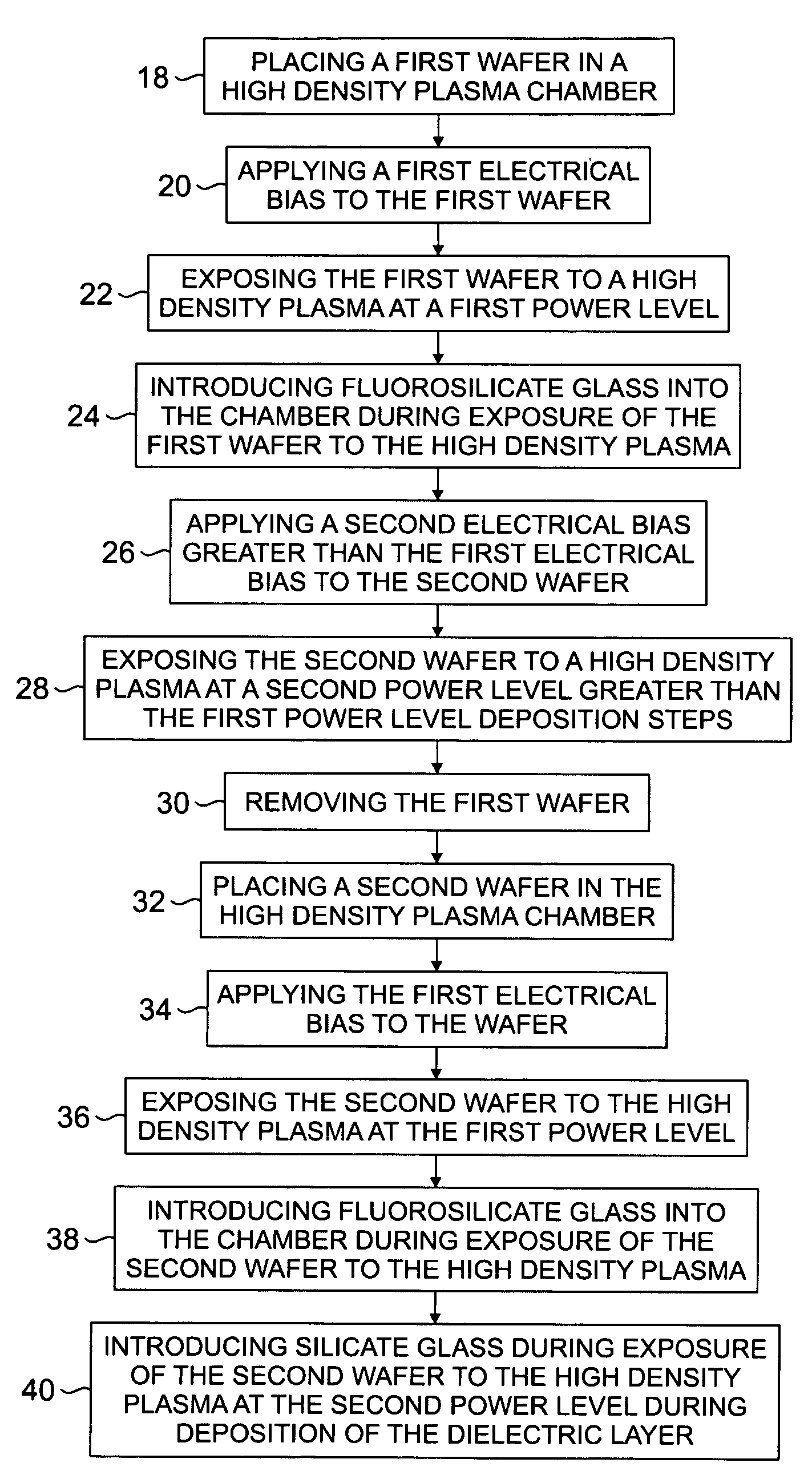
[0018] The inventors have developed innovative solutions for improving throughput in a semiconductor wafer deposition process in a high density plasma chamber by reducing wafer contamination in a fluorinated oxide deposition process, in particular, for a second or additional wafers processed in an HDP chamber after a first wafer has been processed. In one embodiment of the invention, a process for reducing contamination includes exposing the chamber to an oxygen plasma before the second wafer is placed in the chamber. While this method may remove or react with any FSG or free fluorine that has been captured in the material in the chamber, this process may affect a manufacturing process throughput of the chamber because it requires cleaning the chamber after processing each wafer.

[0019] In another embodiment, a process for reducing contamination includes depositing an undoped silicon dioxide film before the second wafer is placed in the chamber. This process simply requires that onc...


PUM

PropertyMeasurementUnit
Densityaaaaaaaaaa

Abstract

A method for improving throughput in a semiconductor wafer deposition process in a high density plasma chamber includes processing a first wafer in the high density plasma chamber using a process that includes high power sufficient to burn fluorosilicate glass residue in the chamber. The method further includes removing the first wafer and processing additional wafers using the same process without cleaning the chamber between wafers.

Description

SPECIFIC DATA RELATED TO THE INVENTION [0001] This application claims benefit of the Feb. 5, 2004 filing date of U.S. provisional application No. 60 / 542,006 and U.S. provisional application No. 60 / 614,665 filed Sep. 30, 2004.FIELD OF THE INVENTION [0002] The present invention relates to semiconductor devices, and, in particular, to a method for reducing semiconductor device contamination problems occurring in a semiconductor device manufacturing process. BACKGROUND OF THE INVENTION [0003] Contamination is a common problem encountered in semiconductor device manufacturing processes. One semiconductor device manufacturing process includes depositing fluorosilicate glass (FSG) on a surface of a multi-layer semiconductor wafer to form an inter-layer dielectric between conductors in the wafer by exposing the wafer to a high density plasma (HDP) comprised of silicon and fluorine containing precursors. The HDP process may include a sputtering deposition and chemical component which typical...

Claims


Application Information

Patent Timeline
IPC IPC(8): C23C16/42B05D1/36B05D7/00C23C14/10C23C16/44H01L21/31H01L21/314H01L21/316H01L21/469H01L21/4763H01L21/768
CPCC23C16/4401C23C16/4404H01L21/76801H01L21/02274H01L21/31629H01L21/02131
Inventor OLMER, LEONARD JAYLAHEY, THOMAS JAMESCAMPBELL, TIMOTHY SCOTTSCHANZER, ROBERT WILLIAMSHUTTLEWORTH, DAVID MARK
Owner AGERE SYST INC
Why Eureka
Try Eureka