Method and architecture for integrated circuit design and manufacture

a technology of integrated circuits and manufacturing methods, applied in the field of integrated circuit design and manufacture, can solve the problems of increasing complexity of chips, increasing cost and risk, and requiring higher performance, so as to achieve cost reduction, cost reduction, and cost reduction

Inactive Publication Date: 2005-09-01
QUALCOMM INC
View PDF7 Cites 28 Cited by
  • Summary
  • Abstract
  • Description
  • Claims
  • Application Information

AI Technical Summary

Benefits of technology

[0040] The various embodiments of the present invention provide many advantages relative to the prior art. One advantage is cost reduction. Because SMPWs are used by multiple users, manufacturing costs are shared and costs are significantly reduced. Another advantage is accessibility to validated IP from the same source, permitting seamless integration of all IPs. Another advantage is seamless market and concept validation, production and risk reduction. Another advantage is frequent manufacturing of the inventive SMPW by the foundries, resulting in enhanced yield. Another advantage is risk elimination due to wide usage and validation of IPs within SMPWs by multiple users. Another advantage is flexibility in assembly and packaging of the customized SMPW die to meet different system requirements and cost structures (i.e., wire-bond, flip chip, BGA, etc.). Another advantage is the flexibility to use different EDA tool sets.

Problems solved by technology

As IC technology advances, the complexity of chips increases and higher performance is required.
In considering an IC design flow, companies face two major issues: cost and risk.
As chip complexity increases, driven by industry SOC migration, the level of risk increases as well.
Development cycles have increased along with the complexity of the ICs, delaying product introduction cycles by 18 months or more.
Market acceptance is a fundamental problem, and can be achieved only by successful chip definition, low cost and short introduction time (time to market).
Price erosion, downward pressure on the cost of IP development, lack of validation and lack of understanding of the overall system have led to serious IP quality issues.
Complex analog blocks are sensitive to their surrounding environments, and analog IP is often developed without an understanding of the environment in which it will be incorporated.
Advanced technologies and high speed signaling result in narrow design margins and, due to validation time and cost, analog IP providers have no means of validating their IP prior to its usage by end users.
It is noteworthy that no analog IP vendor has managed to prove a successful business model.
In 0.13 μm technologies and below, leakage, noise margin, reduced supply voltage and device mismatches have created a new set of design parameters that further complicate design of high performance analog circuits, causing more emphasis to be placed on silicon verified IP and system validitation.
Verification and validation of high performance ICs introduces another risk factor due to system environment and complexity.
While this is a partial answer to the problem, validation increases cycle time and does not address solidity of design over process corners which, in effect, translates to yield.
Moreover, validation of mixed signal IPs by IP vendors is done in a completely different environment and does not eliminate many risk factors.
It is noteworthy that validation of complex IP blocks requires infrastructure, a characterization lab, which is costly and most IP providers do not have.
Before advanced technologies reach a maturation point, process parameters change and, depending on design time, performance and yield problems may manifest themselves.
At present, there are no means for analyzing the yield of acquired IP blocks.
Should IP be acquired from multiple sources, there is no guarantee that different IPs will provide a consistent yield across different manufacturing corners, resulting in serious yield loss at the chip level.
Development cost directly affects market acceptance and profit margins, which in turn drives cost structure and system quality.
Redesign lengthens the development cycle, thereby delaying time to market and increasing cost, resulting in lower profit margins, reduced market acceptance and the possibility of missing the potential market window.
Due to these many cost and risk factors, migration to advanced technologies and SOCs has become a barrier that many companies cannot overcome and has created a roadblock in the industry.
The proposed solutions, discussed below, while addressing some aspects of the problems, fail to provide a platform that addresses all issues.
The shortfalls of FPGAs, however, are in the areas of potential usage, performance and production costs.
Potential usage is limited to the rigid FPGA structure and its pre-defined IP blocks.
Due to the nature of FPGA design, performance is limited and in general only lower frequency ranges can be accommodated.
High production costs prohibit moderate to high volume designs from having competitive ASPs.
Increased cost of development has helped FPGA companies in recent years, such as Xilinx, Altera and so on.
Like FPGAs, however, SAs have a rigid structure that reduces the possibility of their use in productions.
In general, SAs do not provide great added advantage relative to FPGAs and, consequently, have not been the subject of widespread acceptance in the industry.
This may change as cost of development and performance issues take on even greater weight.
The primary issues associated with ASIC flow are the cost of production, which relatively few manufacturers can afford, and the transferability of the finished ASIC to a COT flow (described below).
Along with the high rewards of COT flow comes high risk.
In COT flows, the chip design and integration of IP are not guaranteed to work properly on the first revision of the silicon, as in ASIC flow.
This exposes system houses to a tremendous amount of financial and product introduction risk.
In most cases, in order to get the silicon working properly, system houses must iterate the IC design 1-3 times, which adds development costs and delays product introduction.
The cost of developing an IC via a COT flow requires a significant and costly infrastructure investment.
Hence, the shortcomings of COT flow include acquiring the knowledge for different aspects of the design, acquiring or developing the required IP, management of risk and cost, and inadequate support for concept and market validation, which results in higher risk and potential need for multiple redesigns.
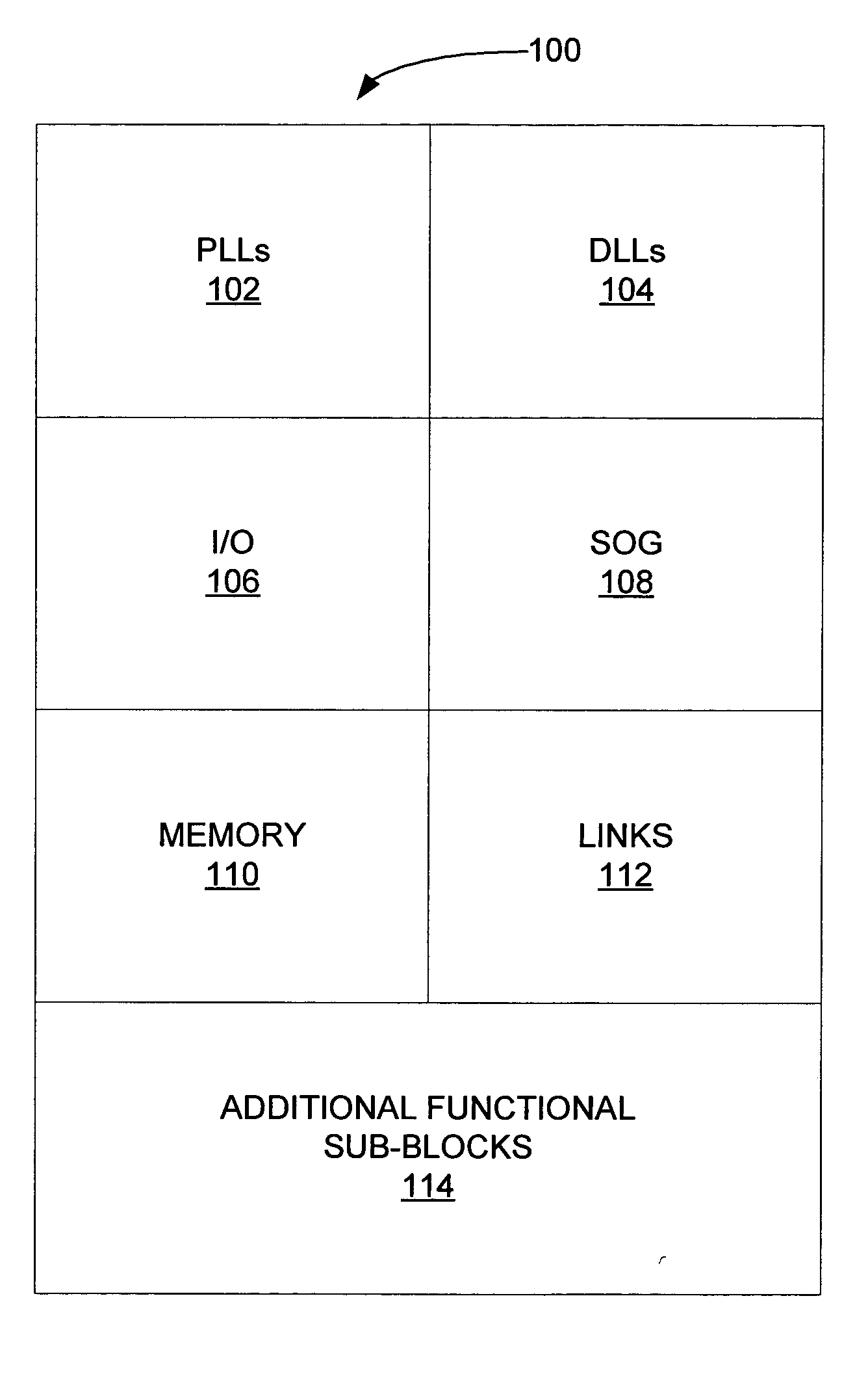
Method used


Image

  • Method and architecture for integrated circuit design and manufacture
  • Method and architecture for integrated circuit design and manufacture
  • Method and architecture for integrated circuit design and manufacture

Examples


Embodiment Construction

[0047] The present invention provides a revolutionary approach to the cost and risk issues surrounding complex IC design and manufacture—a structural multi-project wafer (SMPW). The inventive SMPW comprises multiple pre-manufactured and pre-validated sub-blocks. Each sub-block is targeted to a specific application, function or interface.

[0048] Presently, major fabrication houses provide multi-project wafers (MPWs or shuttles) as test vehicles to their customer base, in which the cost of manufacturing is shared among multiple users, significantly reducing customer manufacturing cost. MPWs or shuttles are used primarily for early system verification or as risk reduction vehicles. The SMPW of the present invention, by contrast, comprises pre-defined structures that are pre-fabricated to the contact level and allows for customization for specific applications. Relative to MPWs, SMPW fabrication time is significantly reduced because they are pre-manufactured to the contact level.

[0049]...


PUM


Abstract

A system for integrated circuit (IC) design. A structural multi-project wafer (SMPW) comprises a plurality of pre-manufactured and pre-validated functional blocks. The SMPW is pre-fabricated up to a contact layer so that a user can customize and program different blocks of the SMPW to the user's requirements. An SMPW provider maintains an inventory of SMPWs. If one of the SMPWs can meet all of a user's IC design requirements, or can serve an intermediate step in a user's IC design process, such as market/concept validation or IP validation, the SMPW is provided to the user. The user can then proceed directly to production using a streamlined design flow having a very short cycle time of 1-3 months. Otherwise, the user proceeds to production using a normal design flow having a much longer cycle time.

Description

FIELD OF THE INVENTION [0001] The present invention relates to integrated circuit (IC) design and manufacture and, in particular, relates to a novel design platform addressing integrated circuit (IC) design and manufacturing issues encountered in sub-micron and advanced technologies. BACKGROUND OF THE INVENTION [0002] As IC technology advances, the complexity of chips increases and higher performance is required. As the industry moves towards a system on a chip model (SoC), uncertainties such as interface requirements and integration of analog blocks must be addressed and resolved. In considering an IC design flow, companies face two major issues: cost and risk. [0003] Cost [0004] Chip design and manufacturing costs for 0.13 μm and 90 nm technologies are estimated to be, respectively in the range of 14 million and 30 million dollars. Costs of this magnitude inhibit many startup companies, and even established companies, from developing products in 0.13 μm and below technologies. Cos...

Claims


Application Information

Patent Timeline
Patent Type & Authority Applications(United States)
IPC IPC(8): G06F17/50
CPCG06F2217/64G06F17/5045G06F2115/06G06F30/30
Inventor MALEKKHOSRAVI, BEHNAMWOODARD, DANIEL J.
Owner QUALCOMM INC
Why Eureka
Try Eureka