Method for fabricating a non-planar nitride-based heterostructure field effect transistor

a heterostructure field effect transistor and nitride-based technology, applied in the direction of semiconductor devices, electrical equipment, basic electric elements, etc., can solve the problems that have not been attainable using gan or other group iii-nitride materials to fabricate non-planar regions, and achieve predictable and repeatable results without reducing the performance of the transistor, prevent oxidation, and prevent damage to the layer of semiconductor materials

Active Publication Date: 2005-09-08
HRL LAB
View PDF10 Cites 6 Cited by
  • Summary
  • Abstract
  • Description
  • Claims
  • Application Information

AI Technical Summary

Benefits of technology

[0009] The present invention provides a transistor having a device structure that allows for the use of dry-etching and wet-etching to create a non-planar region without damaging the transistor. The present invention makes use of the group III-nitride material AlN for creating a non-planar region. AlN has not been used for this application because of the focus on GaN. Because GaN has one of the highest bandgaps of any group III-nitride material, it has been more desirable to find a compatible wet etching process that will work with GaN, than it is to attempt the process with a different group III-nitride material. However, when AlN along with the device structure of the transistor disclosed herein, is processed in conjunction with the wet-etching and dry-etching process disclosed herein, a non-planar region can be fabricated consistently and repeatedly without inducing damage to the rest of the transistor. Such results have not been attainable using GaN or other group III-nitride materials to fabricate non-planar regions in heterostructure field effect transistors.
[0010] It is an object of the present invention to provide a novel method for fabricating a non-planar nitride-based heterostructure field effect transistor. The present invention provides a substrate, whereon at least one layer of semiconductor material is deposited. A layer of AlN is deposited on the at least one layer. An active channel is created at the interface of the AlN layer and the at least one layer. Charges are induced in the channel by both spontaneous polarization and piezoelectric strain at the interface. Furthermore, the at least one layer may further consist of a plurality of laye

Problems solved by technology

Such results have not been attainable using GaN or other group III-nitride mater

Method used


Image

  • Method for fabricating a non-planar nitride-based heterostructure field effect transistor
  • Method for fabricating a non-planar nitride-based heterostructure field effect transistor
  • Method for fabricating a non-planar nitride-based heterostructure field effect transistor

Examples


first embodiment

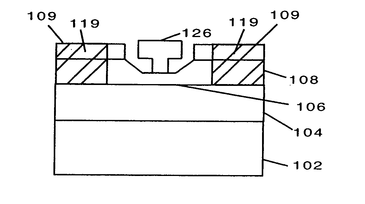
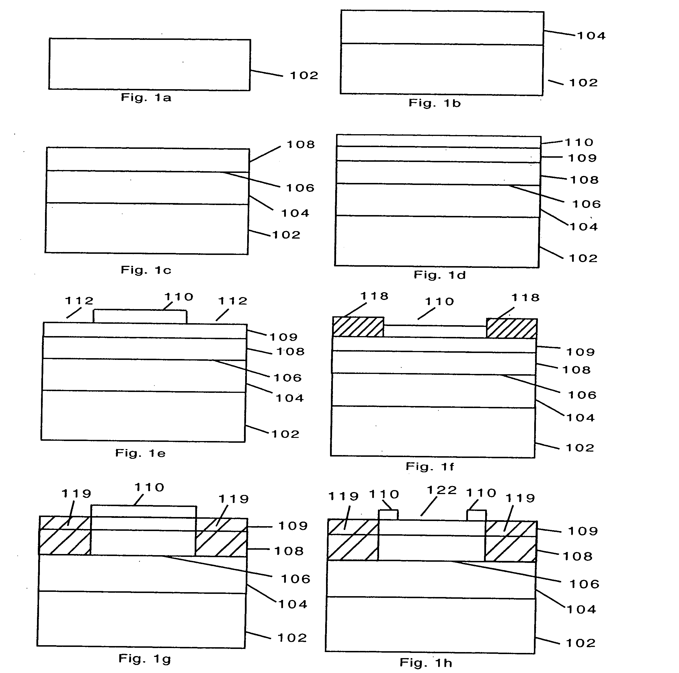
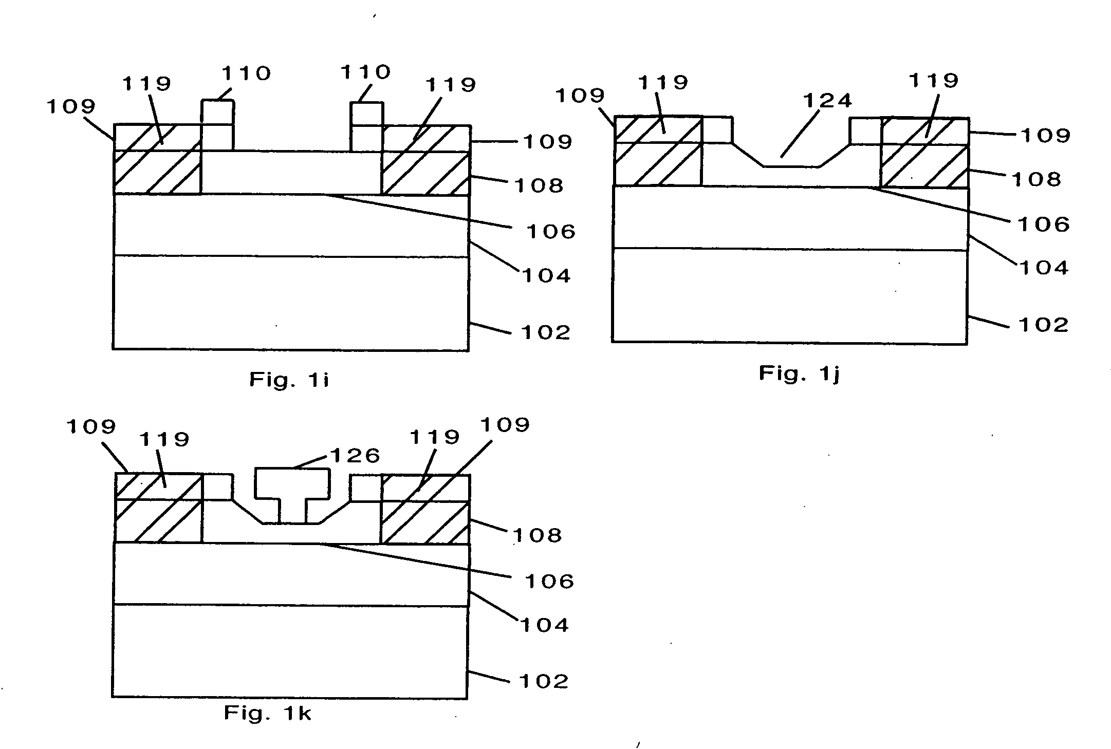
[0050] A method useful for fabricating a non-planar nitride-based heterostructure field effect transistor according to a first embodiment of the present invention is described with reference to FIGS. 1a-1k. In this first embodiment, a substrate 102 is provided as shown in FIG. 1a. The substrate 102 preferably comprises sapphire, silicon carbide, or GaN. Next, a first layer 104 is provided as shown in FIG. 1b. The first layer 104 is deposited, preferably epitaxially, on the substrate 102. The first layer 104 preferably comprises GaN, however other materials such as InP or InGaN can be used as well. Next, an AlN layer 108 is provided as shown in FIG. 1c. The AlN layer 108 is preferably deposited epitaxially on the first layer 104. The AlN layer 108 has a thickness of preferably not more than 10 nm. When the AlN layer 108 is deposited on the first layer 104, an interface 106 is created as shown in FIG. 1c. The interface 106 serves as the channel of the transistor, which will be discuss...

second embodiment

[0055] A method for fabricating a non-planar heterostructure field effect transistor according to a second embodiment of the present invention is described with reference to FIGS. 2a-2m. In this embodiment a substrate 202 as shown in FIG. 2a is provided. The substrate 202 preferably comprises sapphire, silicon carbide, or GaN. A first layer 204 is deposited, preferably epitaxially, on the substrate 202 as shown in FIG. 2b. The first layer 204 preferably comprises GaN, however other materials such as InN or InGaN can be used as well. A second layer 206 is deposited, preferably epitaxially, on the first layer 204. The second layer 206, as shown in FIG. 2c, preferably comprises AlGaN. By depositing the second layer 206 on top of the first layer 204, an interface 208 is created. The interface 208 is located where the first layer 204 contacts the second layer 206 and is further discussed later. A third layer 210 is deposited, preferably epitaxially, on the surface of the second layer 206...

third embodiment

[0061] A method for fabricating a non-planar heterostructure field effect transistor according to a third embodiment is described with reference to FIGS. 3a-3l. In this embodiment, a substrate 302 is provided as shown in FIG. 3a. The substrate 302 preferably comprises sapphire, silicon carbide, or GaN. Next, a first layer 304 preferably comprising GaN is provided as shown in FIG. 3b, however, other materials such as InN or InGaN could work equally as well. The first layer 304 is deposited, preferably epitaxially, on the substrate 302. A second layer 306 is provided as shown in FIG. 3c. The second layer 306 preferably comprises AlGaN and is deposited, preferably epitaxially, on the first layer 304. By depositing the second layer 306 on the first layer 304, an interface 305 is created. The interface 305 is located where the first layer 304 contacts the second layer 306 and is further discussed later. Next, an AlN layer 308 is deposited, preferably epitaxially on the second layer 306 a...


PUM


Abstract

A method for fabricating a non-planar heterostructure field effect transistor using group III-nitride materials with consistent repeatable results is disclosed. The method provides a substrate on which at least one layer of semiconductor material is deposited. An AlN layer is deposited on the at least one layer of semiconductor material. A portion of the AlN layer is removed using a solvent to create a non-planar region with consistent and repeatable results. The at least one layer beneath the AlN layer is insoluble in the solvent and therefore acts as an etch stop, preventing any damage to the at least one layer beneath the AlN layer. Furthermore, should the AlN layer incur any surface damage as a result of the reactive ion etching, the damage will be removed when exposed to the solvent to create the non-planar region.

Description

CROSS-REFERENCE TO RELATED APPLICATIONS [0001] This application is related to and claims benefit of U.S. Provisional Application 60 / 411,076 filed on Sep. 16, 2002, which is incorporated by reference in its entirety.FIELD OF THE INVENTION [0002] The present invention relates to a method for fabricating a semiconductor structure useful for fabricating a non-planar heterostructure field effect transistor. More specifically, the present invention relates to a method for fabricating a semiconductor structure useful for fabricating a non-planar nitride-based heterostructure field effect transistor, wherein the non-planar region is fabricated in the group III-nitride material aluminum nitride (AlN) and the semiconductor structure is not damaged by dry etching or wet etching. BACKGROUND OF THE INVENTION [0003] The use of group III-nitride substrates has become popular for fabricating a non-planar region in a non-planar heterostructure field effect transistor. A non-planar heterostructure fi...

Claims


Application Information

Patent Timeline
IPC IPC(8): H01L21/285H01L21/306H01L21/335H01L29/20H01L29/778
CPCH01L21/28587H01L21/30612H01L29/7787H01L29/66462H01L29/2003
Inventor MOON, JEONG SUNHASHIMOTO, PAULWONG, WAH S.GRIDER, DAVID E.
Owner HRL LAB
Why Eureka
Try Eureka