Single-chip white light emitting device

Active Publication Date: 2005-09-08
GENESIS PHOTONICS
View PDF2 Cites 39 Cited by
  • Summary
  • Abstract
  • Description
  • Claims
  • Application Information

AI Technical Summary

Benefits of technology

[0015] In addition, to further enhance the CRI index and the color temperature modulation capability in terms of red light, the single-chip white light emitting device according to this invention may be added with red fluorescent powder of an appropriate amount to be packaged together for attaining a white light emitting device with three wavelength spectrums. The addition of the red fluorescent powder mainly intends to enhance the weaker

Problems solved by technology

However, with the blue halo effect, the reducing reliability and low light conversion efficiency of fluorescent powder, and the limited characteristics of fluorescent powder, such a structure cannot attain white light emitting devices with high color saturation, high luminous intensity, high reliability and capable of various color temperature modulation.
Such a structure involves the drawbacks of poor reliability in the mixture of RGB fluorescent powder.
In addition, the light source generated from exciting UVA cannot serve as a mixed light source, thereby resulting in an even lower luminous intensity.
However, the commercially available package attained from such a structure is limited to that including red-orange-yellow light AlGaInP LED and nitrides blue LED with a wavelength greater than 580 nm.
As such, the drawbacks of such a structure include the high cost involved in packaging multiple chips, and dif

Method used


Image

  • Single-chip white light emitting device
  • Single-chip white light emitting device
  • Single-chip white light emitting device

Examples


first embodiment

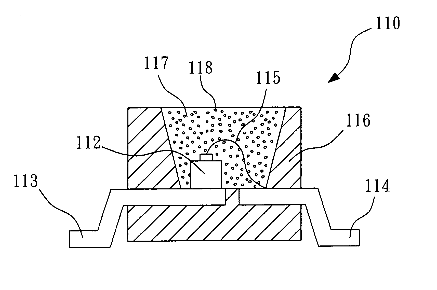
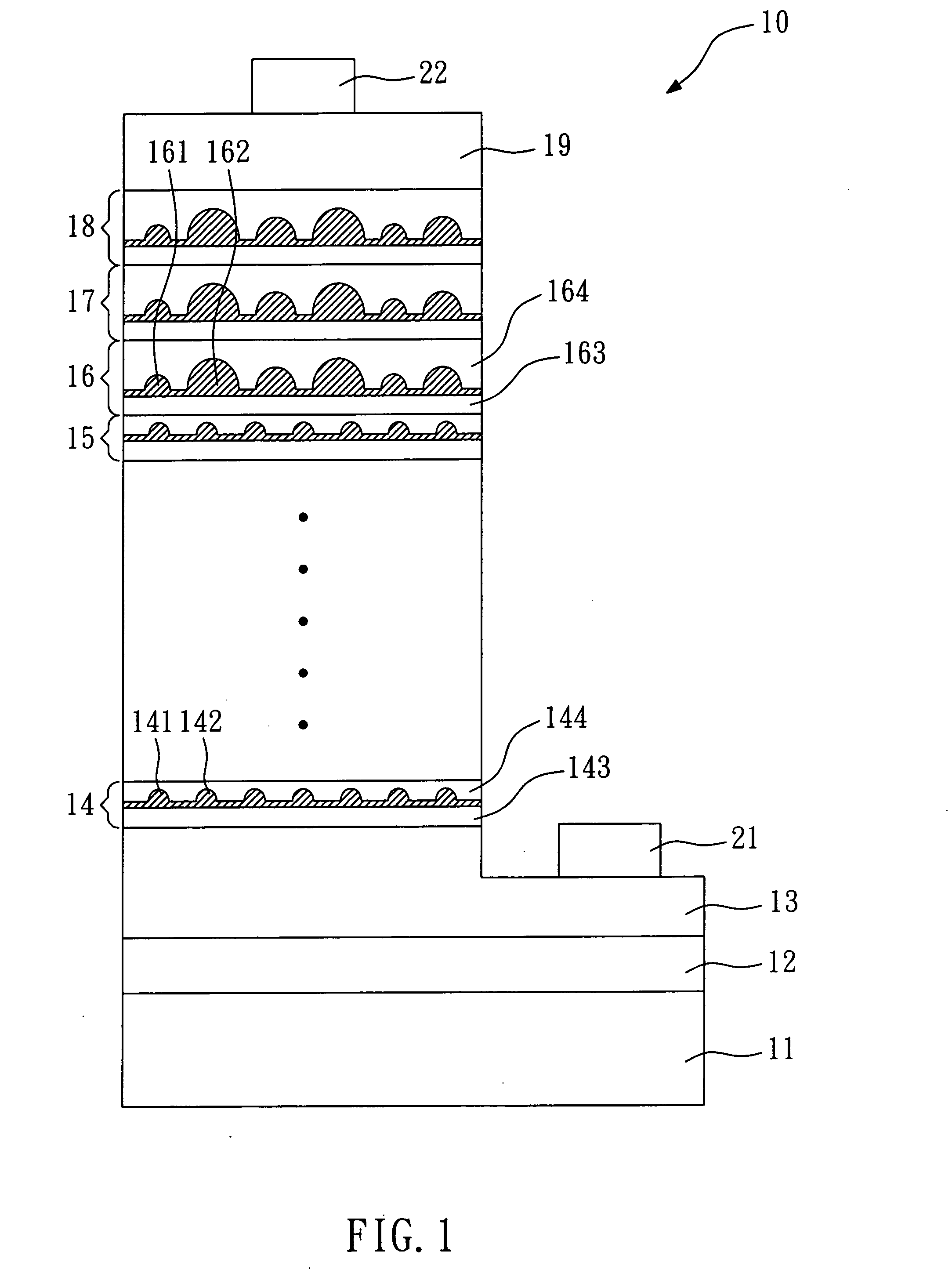
[0030]FIG. 1 is a schematic view illustrating the laminar structure of a single-chip white light emitting device 10 according to this invention. The single-chip white light emitting device 10 comprises: a substrate 11, a buffer layer 12, a first conductive cladding layer 13, seven blue light quantum dot emitting layer 14, 15, three broad-spectrum blue-complimentary light quantum dot emitting layers 16, 17, 18 and a second conductive cladding layer 19. The single-chip white light emitting device 10 further comprises two electrodes 21, 22 to be connected to an external power source. The buffer layer 12 is disposed over the substrate. The first conductive cladding layer 13 is disposed over the buffer layer 12. The first conductive cladding layer 13 may be an N-type cladding layer and serves to supply electrons. The second conductive cladding layer 19 is disposed over he quantum dot emitting layer 18. The first conductive cladding layer 19 may be a P-type cladding layer and serves to su...

second embodiment

[0038] As shown in FIG. 3, the single-chip white light emitting device 30 according to this invention is provided between the first and second conductive cladding layers 13, 19 with six broad-spectrum blue-complimentary light quantum dot emitting layers 31, 33 and four blue light quantum dot emitting layers 34, 35, 36, 37. The six broad-spectrum blue-complimentary light quantum dot emitting layers 31, 33 are sequentially disposed over the first conductive cladding layer 13. The broad-spectrum blue-complimentary light quantum dot emitting layers each have plural quantum dots. As exemplified by the broad-spectrum blue-complimentary light quantum dot emitting layer 31, the broad-spectrum blue-complimentary light quantum dot emitting layer 31 includes plural quantum dots 311, 312 and two barrier layers 313, 314, where each layer includes quantum dots of different dimensions to result in an uneven character distribution of the quantum dots, so as to increase FWHM of the emission waveleng...

third embodiment

[0042] With reference to FIG. 5, a single-chip white light emitting device 50 according to this invention is provided between the first and second conductive cladding layers 13, 19 with nine broad-spectrum blue-complimentary light quantum dot emitting layers 51, 53 and a broad-spectrum blue light quantum dot emitting layer 54. The nine broad-spectrum blue-complimentary light quantum dot emitting layers 51, 53 are sequentially disposed over the first conductive cladding layer 13. The broad-spectrum blue-complimentary light quantum dot emitting layers each include plural quantum dots. As exemplified by the broad-spectrum blue-complimentary light quantum dot emitting layer 51, the broad-spectrum blue-complimentary light quantum dot emitting layer 51 includes plural quantum dots 511, 512 and two barrier layers 513, 514, where each layer includes quantum dots of different dimensions to result in an uneven character distribution of the quantum dots, so as to increase FWHM of the emission ...


PUM


Abstract

A single-chip white light emitting device, including: a substrate, a buffer layer, a first conductive cladding layer, a second conductive cladding layer, at least one broad-spectrum blue-complimentary light quantum dot emitting layer and at least one blue light emitting layer. The buffer layer is disposed over the substrate. The first conductive cladding layer is disposed over the buffer layer. The broad-spectrum blue-complimentary light quantum dot emitting layer is disposed between the first conductive cladding layer and the second conductive cladding layer. The blue-complimentary light quantum dot emitting layer includes plural quantum dots with an uneven character distribution, so as to increase FWHM of emission wavelength of the quantum dot emitting layer. The blue light emitting layers is disposed between the first and second conductive cladding layers, such that mixing of blue light and blue-complimentary light would generate white light. According to the single-chip white light emitting device of this invention, a single LED laminar structure is provided therein with a broad-spectrum blue-complimentary light quantum dot emitting layer and a blue light emitting layer, which are mixed to form an Al(1-x-y)InyGaxN single-chip white light emitting device with a high CRI, and high emission and are capable of color temperature modulation.

Description

FIELD OF THE INVENTION [0001] The invention relates to a white light emitting device, particularly to a single-chip white light emitting device. BACKGROUND OF THE INVENTION [0002] The rapid development of nitrides emitting devices in recent years has resulted in high demands in high brightness LED. Along with the significant enhancement in emission efficiency, high interest and expectation are given to the use of high brightness LED to serve as a white light source. Presently, the structures using high brightness LED to serve as white light sources include the followings: [0003] The first structure is developed by Nichia Kagaku Kogyo Kabushiki Kaisha, where yellow fluorescent powder (YAG: Ce; Y3Al5O12: Ce3+) is added into blue LED to generate mixed white light (with reference to U.S. Pat. No. 6,069,440). Such a structure provides a white light emitting device that is of the lowest cost among the commercially available white light emitting devices. However, with the blue halo effect,...

Claims


Application Information

Patent Timeline
IPC IPC(8): H01L29/20H01L33/00
CPCB82Y10/00
Inventor CHEN, CHENG CHUAN
Owner GENESIS PHOTONICS
Why Eureka
Try Eureka