Method for mounting semiconductor chips and corresponding semiconductor chip system

a technology of semiconductor chips and mounting methods, applied in the direction of semiconductor/solid-state device details, instruments, soldering apparatus, etc., to achieve the effect of simple, cost-effective, and insensitive to stress

Inactive Publication Date: 2005-09-08
ROBERT BOSCH GMBH
View PDF2 Cites 49 Cited by
  • Summary
  • Abstract
  • Description
  • Claims
  • Application Information

AI Technical Summary

Benefits of technology

[0007] The method according to the present invention for mounting semiconductor chips and the corresponding semiconductor chip system

Problems solved by technology

However, such a construction has the disadvantage that it is cumbersome, and that problems frequently arise with the hermetic enclosing of sensor chip 5, for instance, because of leaky welding seams or the like.
When s

Method used


Image

  • Method for mounting semiconductor chips and corresponding semiconductor chip system
  • Method for mounting semiconductor chips and corresponding semiconductor chip system
  • Method for mounting semiconductor chips and corresponding semiconductor chip system

Examples


Embodiment Construction

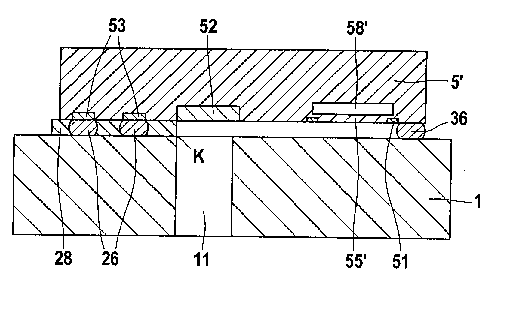
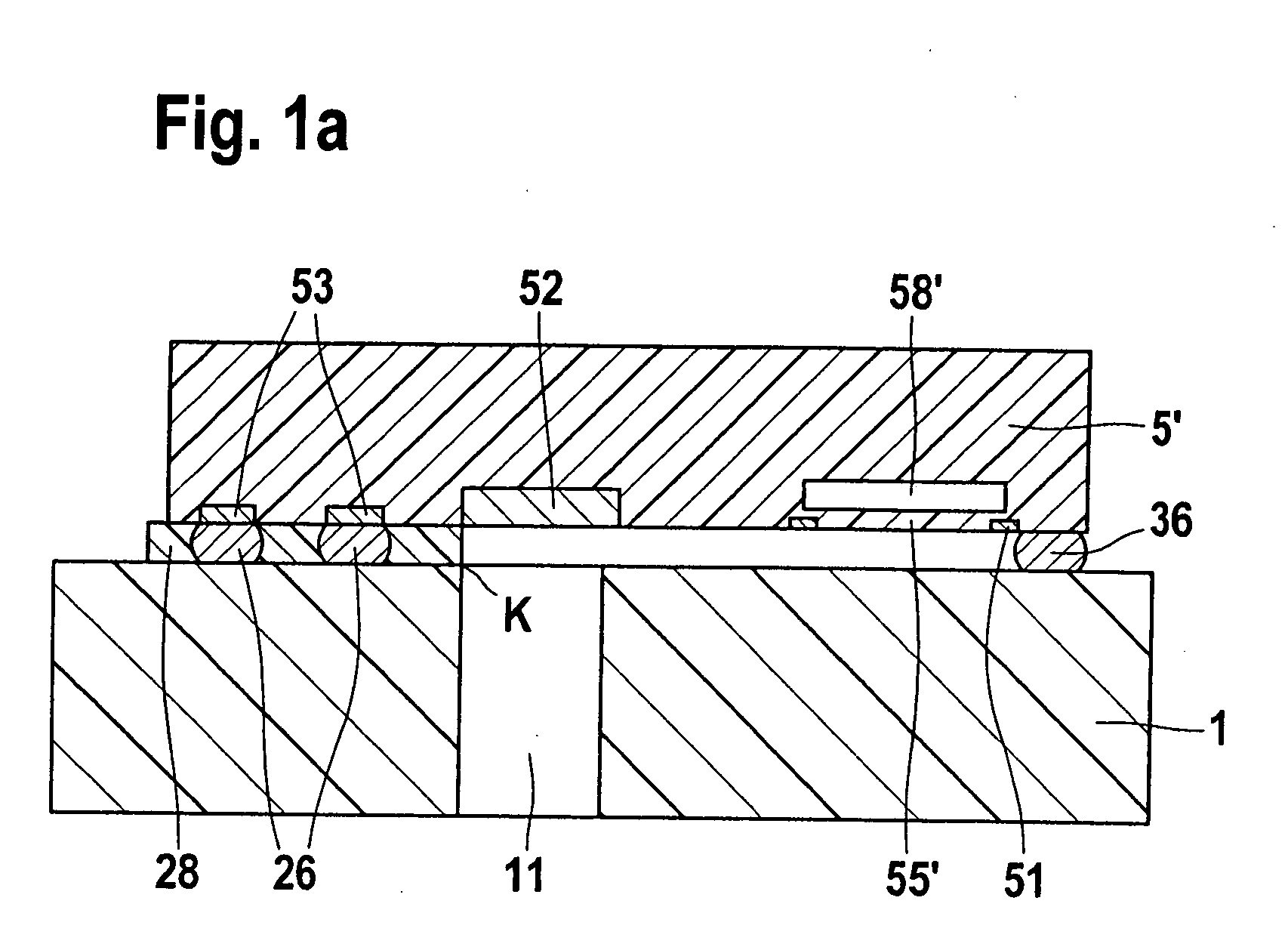
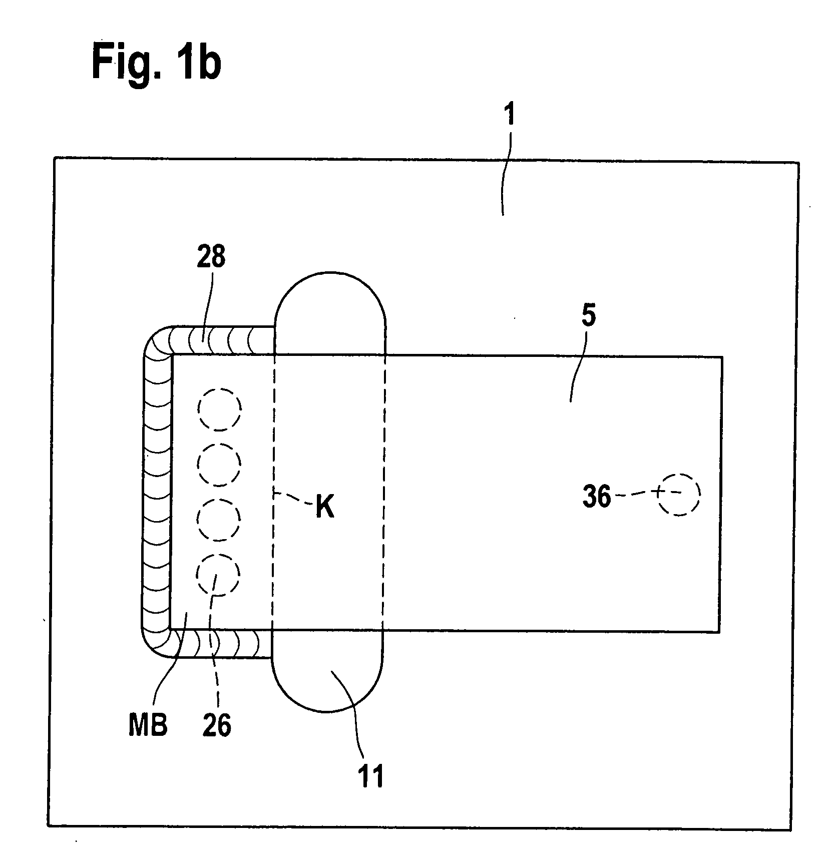
[0027] In the figures discussed below, identical reference numerals denote identical or functionally identical components.

[0028]FIGS. 1a and 1b illustrate a first example embodiment of the method according to the present invention for mounting semiconductor chips and a corresponding semiconductor chip system (FIG. 1a shows a side-plane cross-sectional view, and FIG. 1b shows a top-plane cross sectional view).

[0029] In the first example embodiment shown in FIGS. 1a and 1b, sensor chip 5′ is a surface micromechanical sensor chip which is produced, for example, according to the method described in German patent document DE 100 32 579, and which sensor chip has an integrated cavity 58′ above a diaphragm region 55′.

[0030] Substrate 1 has a recess 11, next to which sensor chip 5′ is mounted in flip-chip technique in an overhanging fashion. For the mounting, bondpads 53 of sensor chip 5′ are soldered in mounting region MB onto bondpads of substrate 1, using a solder or adhesive connecti...


PUM

PropertyMeasurementUnit
Areaaaaaaaaaaa

Abstract

A method for mounting semiconductor chips includes the steps of: a) providing a semiconductor chip having a surface that has a diaphragm region and a peripheral region, the peripheral region having a mounting region; b) providing a substrate which has a surface having a recess; c) mounting the mounting region of the semiconductor chip using a flip-chip technique onto the surface of the substrate in such a way that an edge of the recess lies between the mounting region and the diaphragm region; and d) underfilling the mounting region using an underfilling component, the edge of the recess being used a demarcation region for the underfilling component, so that no underfilling component is able to get into the diaphragm region. Also provided is a corresponding semiconductor chip system.

Description

FIELD OF THE INVENTION [0001] The present invention relates to a method for mounting semiconductor chips and a corresponding semiconductor chip system. BACKGROUND INFORMATION [0002]FIG. 7 shows a conventional method of mounting semiconductor chips and a corresponding semiconductor chip system in cross sectional view. In FIG. 7, reference numeral 100 denotes a TO8 base produced, for example, from Kovar. Reference numeral 5 is a micromechanical silicon pressure-sensor chip having piezoresistive transformer elements 51 that are accommodated on a diaphragm 55. To produce diaphragm 55, a cavity 58 is introduced onto the back of respective silicon pressure sensor chip 5, for instance, by anisotropic etching, e.g., using KOH or TMAH. Alternatively, diaphragm 55 may also be produced by trench-etching. [0003] Sensor chip 5 may be made up of a pure resistance bridge having piezoresistive resistors, or may be combined with an evaluation circuit which is integrated, together with the piezoresis...

Claims


Application Information

Patent Timeline
IPC IPC(8): G01L9/00B81B7/00B81C3/00H01L21/48H01L21/60H01L23/48H01L29/84
CPCB81B7/0048B81B2201/0257H01L2924/00013H01L2224/131H01L2224/1715H01L2224/29035H01L2924/014H01L2924/01068H01L2924/01033H01L2924/01019H01L2924/01006H01L2924/01005H01L2924/01082H01L2224/73204G01L19/148B81B2207/012G01L19/0636G01L19/141G01L19/145H01L2224/13099H01L2224/13599H01L2224/05599H01L2224/05099H01L2224/29099H01L2224/29599H01L2224/05571H01L2224/05573H01L2924/00014
Inventor WEIBLEN, KURTBENZEL, HUBERTGROTE, REGINA
Owner ROBERT BOSCH GMBH
Why Eureka
Try Eureka