Solvents and methods using same for removing silicon-containing residues from a substrate

a technology of silicon-containing residues and solvents, applied in the field of microelectronics, can solve the problems of significant amount of silicon-containing residues being deposited onto the deposition apparatus itself, poor image focus, and insufficient removal of at least a portion of silicon

Inactive Publication Date: 2005-09-08
AIR PROD & CHEM INC
View PDF24 Cites 7 Cited by
  • Summary
  • Abstract
  • Description
  • Claims
  • Application Information

AI Technical Summary

Problems solved by technology

The aforementioned solvents, however, may be inadequate to remove at least a portion of a silicon-containing film that is deposited onto a substrate and / or the deposition apparatus.
In this connection, residue present on the back side of the substrate may be detrimental to processing because of contamination to hot plates and / or poor substrate contact with the stepper chucks, i.e., chucks that hold the substrate during lithography, resulting in poor image focus.
Moreover, a significant amount of silicon-containing residue may be deposited onto the deposition apparatus itself, such as the interior of the deposition apparatus, during the dispensing, leveling, and / or drying of the film portion of the deposition process.
These particles may cause visible defects in the film such as comet trails, holes, and striations.
If these particles are incorporated into the as-deposited film, the defects may result in poor imaging during lithography, different etch rates, failure during CMP, barrier defects, shorting between metal lines, and device failure.

Method used


Image

  • Solvents and methods using same for removing silicon-containing residues from a substrate
  • Solvents and methods using same for removing silicon-containing residues from a substrate
  • Solvents and methods using same for removing silicon-containing residues from a substrate

Examples


examples

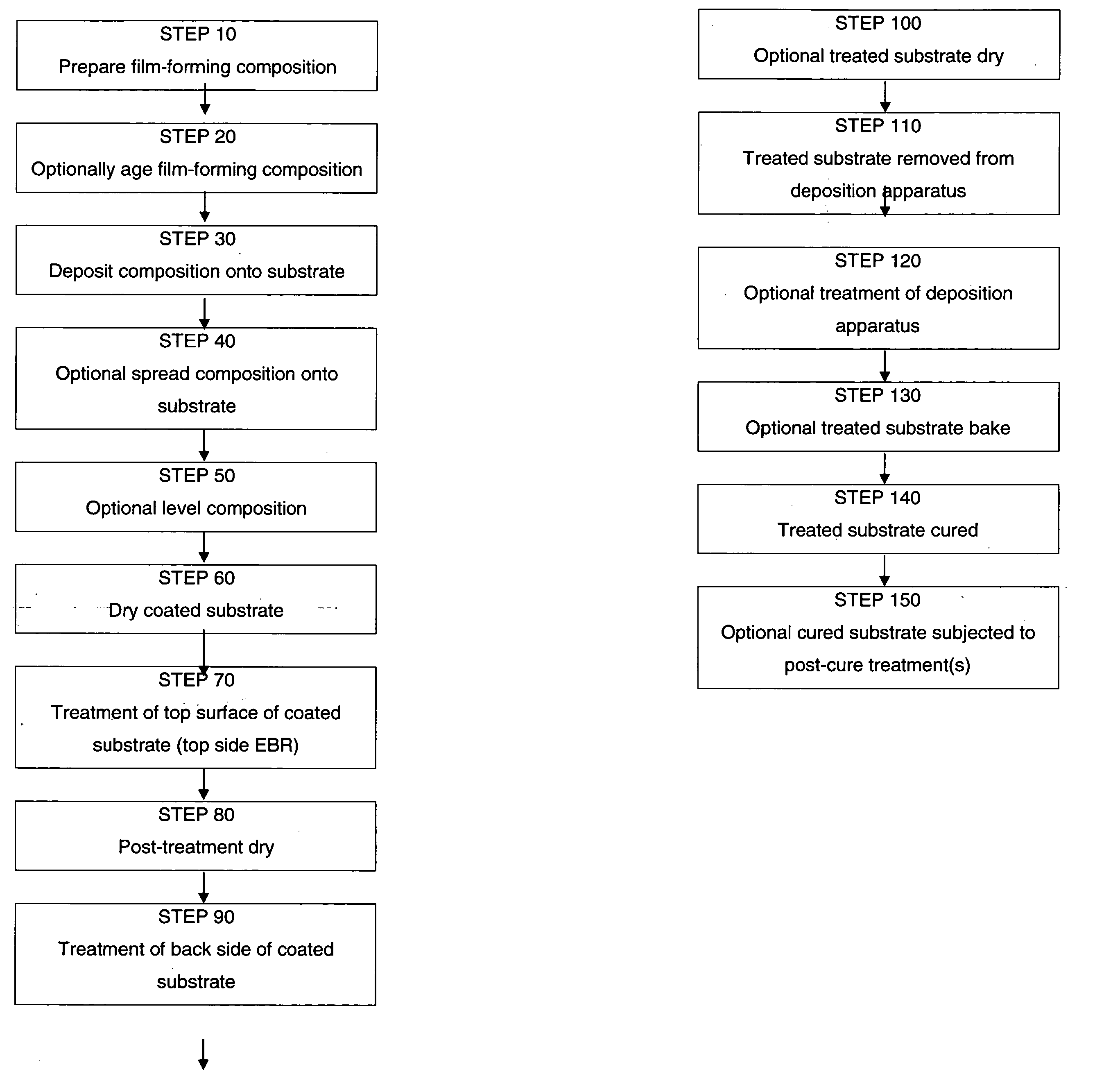
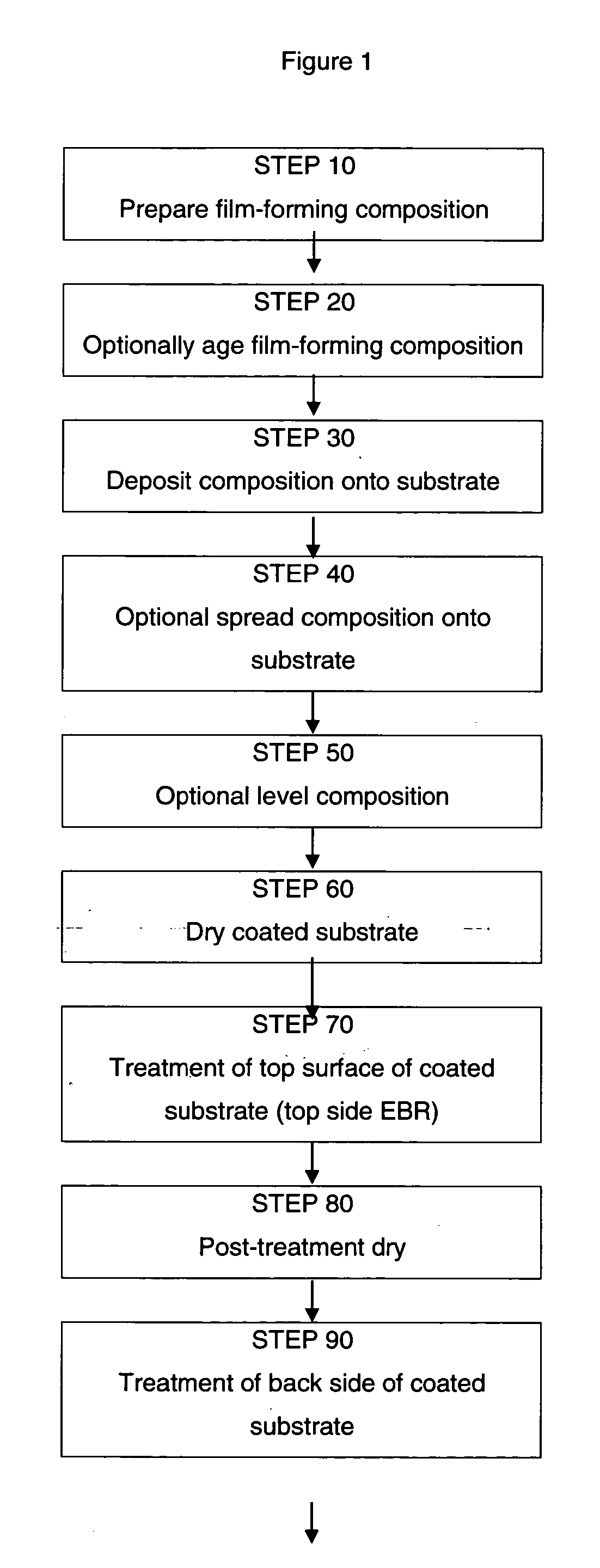
[0053] In the following examples, unless stated otherwise, properties were obtained from sample films that were spun onto a low resistance (0.01 Ωcm) single crystal silicon substrate and heated to 400° C. For the thickness values, the error between the simulated thickness and actual film thickness values measured by profilometry was generally less than 2%. Uniformity across 200 and 300 mm substrates was performed on a Rudolph Model # Focus Fe IV-D spectroscopic ellipsometer tool using a standard 49 point substrate map.

[0054] Surface tension is measured using the Wilhelmy plate method on a Kruss Digital Tensiometer # K10ST. A vertical plate, typically made of platinum of know perimeter is attached to a balance and the force due to wetting is measured using a digital tensiometer as the plate is lowered into the film-forming composition.

[0055] Viscosity measurements were performed using a SR5 controlled stress rheometer from Texas Instruments. All measurements were made at 25° C.; te...


PUM

PropertyMeasurementUnit
viscosityaaaaaaaaaa
temperatureaaaaaaaaaa
surface tensionaaaaaaaaaa

Abstract

A method for the removal of residues comprising silicon from at least a portion of the top and back of a substrate and/or deposition apparatus is disclosed herein. In one aspect, there is provided a method for removing residues comprising: treating the coated substrate and/or deposition apparatus with a removal solvent.

Description

CROSS-REFERENCE TO RELATED APPLICATIONS [0001] This application claims the benefit of U.S. Provisional Application No. 60 / 549,251, filed 2 Mar. 2004.BACKGROUND [0002] There is a continuing desire in the microelectronics industry to increase the circuit density in multilevel integrated circuit devices such as memory and logic chips in order to improve the operating speed and reduce power consumption. In order to continue to reduce the size of devices on integrated circuits, it has become necessary to use insulators having a low dielectric constant to reduce the resistance-capacitance (“RC”) time delay of the interconnect metallization and to prevent capacitive cross talk between the different levels of metallization. Such low dielectric materials are desirable for premetal dielectric layers and interlevel dielectric layers. [0003] Typical dielectric materials for devices with 180 nm line width are materials with a dielectric constant between about 3.8 and 4.2. As the line width decre...

Claims


Application Information

Patent Timeline
Patent Type & Authority Applications(United States)
IPC IPC(8): B05D3/00H01L21/31H01L21/306H01L21/3213
CPCC11D7/266C11D11/0047H01L21/02126H01L21/02203H01L21/02216H01L21/31695H01L21/02337H01L21/02343H01L21/3121H01L21/3122H01L21/3124H01L21/02282B24B23/005B24B3/38B27G17/00
Inventor WEIGEL, SCOTT JEFFREYKHOT, SHRIKANT NARENDRAMORRIS-OSKANIAN, ROSALEEN PATRICIAMAYORGA, STEVEN GERARDMAC DOUGALL, JAMES EDWARDSENECAL, LEE
Owner AIR PROD & CHEM INC
Why Eureka
Try Eureka