Electron beam exposure system

a technology of electron beam and exposure system, which is applied in the field of electron beam exposure system, can solve the problems of correction value, homogeneity of beamlets, and limited system output, and achieve the effect of improving the performance of known electron beam exposure apparatus

Inactive Publication Date: 2005-09-29
ASML NETHERLANDS BV
View PDF5 Cites 50 Cited by
  • Summary
  • Abstract
  • Description
  • Claims
  • Application Information

AI Technical Summary

Benefits of technology

[0009] It is an objective of the current invention to improve the performance of known electron beam exposure apparatus.
[0010] Another objective is to improve the resolution of known electron beam exposure apparatus.
[0011] Yet another objective of the current invention is to improve throughput of known electron beam exposure apparatus.

Problems solved by technology

The throughput of this system is still limited.
As all these emitters have slightly different emission characteristics, homogeneity of the beamlets is a problem.
Correction values for the mismatch are extremely difficult to calculate and it takes a significant amount of time, which reduces the throughput of the system.
A major disadvantage of this approach is that the plurality of electron beamlets together has to pass through at least one complete crossover.
In this crossover, Coulomb interactions between electron in different beamlets will disturb the image, thus reducing the resolution.
Furthermore, controlling individual sub-beams is a problem, and maintaining inter-sub-beam uniformity.
A disadvantage of such a source is its limited output.
Furthermore, the intensity of the source is a problem.
A further problem, not recognised in this publication, is correction of deviation of electron beamlets from their intended positions.

Method used


Image

  • Electron beam exposure system
  • Electron beam exposure system
  • Electron beam exposure system

Examples


first embodiment

[0087] In a first embodiment, shown in FIG. 3, crossover in the illumination electron optics is avoided by using an electron source 1 with a spherical or a hemispherical outer surface 15. In this configuration a large opening angle α is formed, which reduces the blur due to electron-electron interactions in the emitted electron beam 5. Additionally the electron beams are forming a spherical wave front, which results in a virtual crossover 16 located in the centre of the source. There are no electrons present in the virtual crossover; so disturbing electron-electron interactions are absent.

[0088] The electrons can be extracted with a spherical extractor that comprises large holes. The main advantage of the spherical shape of the extractor is the more homogeneous field that is created.

[0089] In an alternative embodiment, shown in FIG. 3A, crossover is avoided by extracting the electrons from the source / cathode 1 which is at a voltage Vs and has a distant planar extractor 11. The plan...

second embodiment

[0103] In a second embodiment, the electrostatic scan deflectors 18 are located on the protective means.

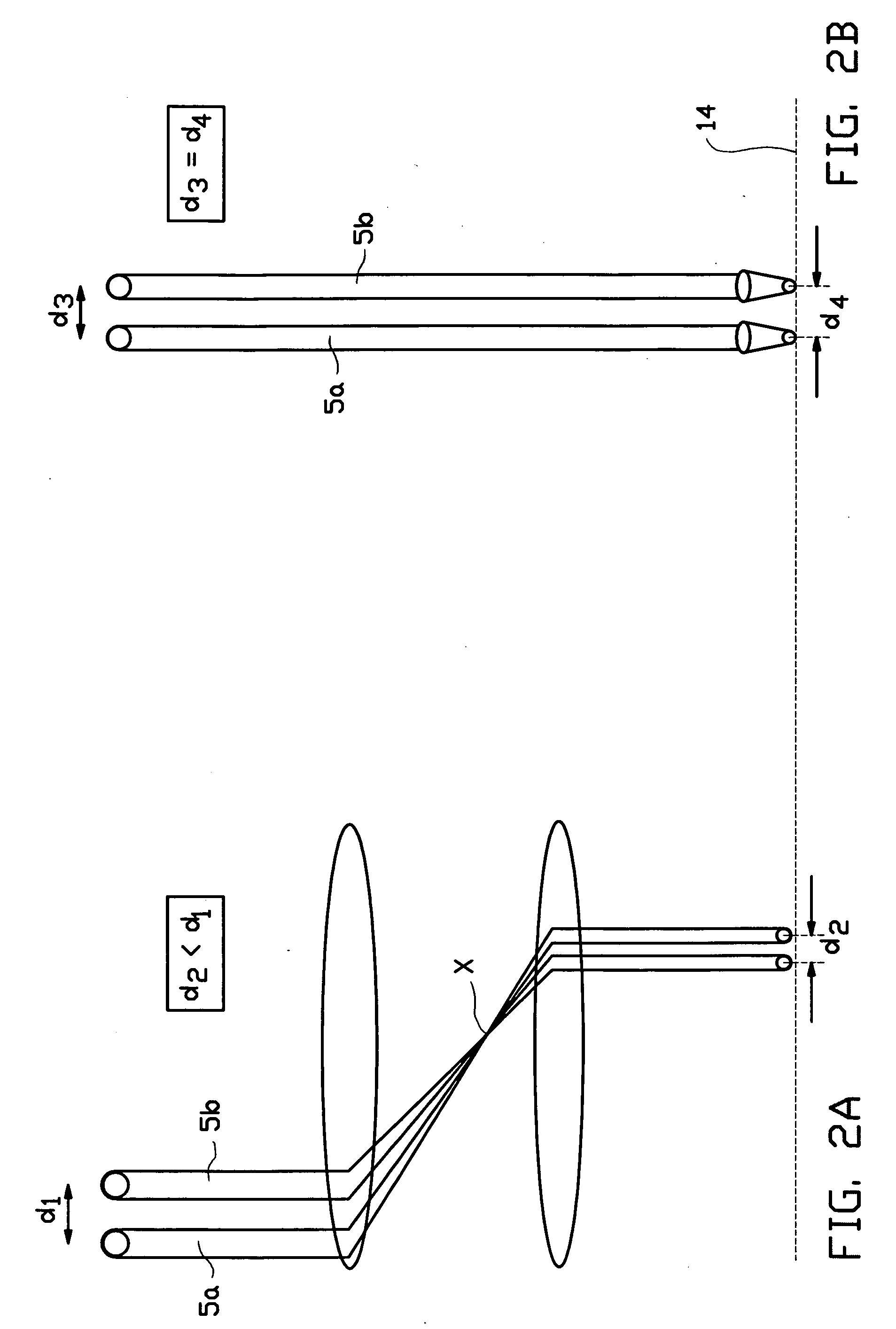
[0104] The electrostatic scan deflectors 18 comprise scan deflection electrodes, which are arranged to deflect an assembly of electron beamlets in the same direction. The scan deflection electrodes may be deposited in the form of strips 19 on a suitable plate 20 at the target exposure surface side as is shown in FIG. 5A. The best yield can be established when the strips 19 are deposited close to the beamlet, thus close to the aperture 21, since this reduces db-sd. Moreover, it is preferable to position the scan deflection electrodes outside an individual beamlet crossover plane.

[0105] In one embodiment the first assembly is scanned in one direction while the next one is scanned in the opposite direction, by putting alternating voltages on the consecutive strips 19 as is shown in FIG. 5B. The first strip has for instance a positive potential, the second one a negative potential, t...


PUM


Abstract

The invention relates to an electron beam exposure apparatus for transferring a pattern onto the surface of a target, comprising: a beamlet generator for generating a plurality of electron beamlets; a modulation array for receiving said plurality of electron beamlets, comprising a plurality of modulators for modulating the intensity of an electron beamlet; a controller, connected to the modulation array for individually controlling the modulators, an adjustor, operationally connected to each modulator, for individually adjusting the control signal of each modulator; a focusing electron optical system comprising an array of electrostatic lenses wherein each lens focuses a corresponding individual beamlet, which is transmitted by said modulation array, to a cross section smaller than 300 nm, and a target holder for holding a target with its exposure surface onto which the pattern is to be transferred in the first focal plane of the focusing electron optical system.

Description

BACKGROUND [0001] Several kinds of electron beam exposure systems are known in the art. Most of these systems are provided to transfer very precise patterns onto an exposure surface of a substrate. Since lithography features are pushed to become smaller and smaller following Moore's law, the high resolution of electron beams could be used to continue the drive to even smaller features than today. [0002] A conventional electron beam exposure apparatus has a throughput of about 1 / 100 wafer / hr. However, for lithography purposes a commercially acceptable throughput of at least a few wafers / hr is necessary. Several ideas to increase the throughput of an electron beam exposure apparatus have been proposed. [0003] U.S. Pat. No. A1-5,760,410 and U.S. Pat. No. A1-6,313,476, for instance, disclose a lithography system using an electron beam having a cross section, which is modified during the transferring of a pattern to an exposure surface of a target. The specific cross section or shape of ...

Claims


Application Information

Patent Timeline
Patent Type & Authority Applications(United States)
IPC IPC(8): A61N5/00G01Q30/02G01Q30/08G03B1/00H01J37/08H01J37/30H01J37/304H01J37/317
CPCB82Y10/00B82Y40/00H01J3/02H01J2237/3045H01J37/3177H01J2237/0435H01J37/06H01J2237/06308H01J2237/06375H01J37/302H01J37/304H01J37/317
Inventor WIELAND, MARCO JAN-JACOKAMPHERBEEK, BERT JANVINCENT VAN VEEN, ALEXANDER HENDERIKKRUIT, PIETER
Owner ASML NETHERLANDS BV
Why Eureka
Try Eureka