Multi-layer printed circuit board transformer winding

Inactive Publication Date: 2005-09-29
ASTEC INT LTD
View PDF6 Cites 81 Cited by
  • Summary
  • Abstract
  • Description
  • Claims
  • Application Information

AI Technical Summary

Benefits of technology

[0009] The present invention solves the above-identified problems of windings formed by multi-layer PCBs. In particular, a winding is provided for an electromagnetic component that is formed from a combination of multi-layer PCB conductive traces and one or two additional conducting layers,

Problems solved by technology

The resulting components are expensive and time consuming to manufacture, and do not readily lend themselves to miniaturization or automated assembly.
It is a well known problem of prior art power chokes formed using layers of stacked metal foils separated by insulators that shorting between layers is much more likely to occur.
Windings constructed from two or more conducting layers of a multi-layer PCB have many advantages over conventional wire windings, but have problems that result from the structure of PCBs.
One problem with multi-layer PCB windings results from their having thin conducting layers separated by insulating

Method used


Image

  • Multi-layer printed circuit board transformer winding
  • Multi-layer printed circuit board transformer winding
  • Multi-layer printed circuit board transformer winding

Examples


Embodiment Construction

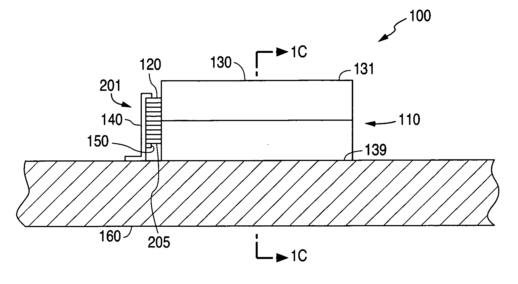
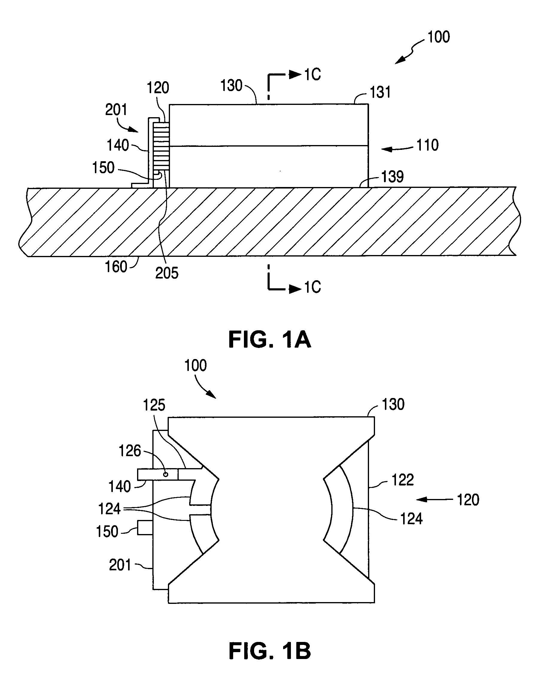
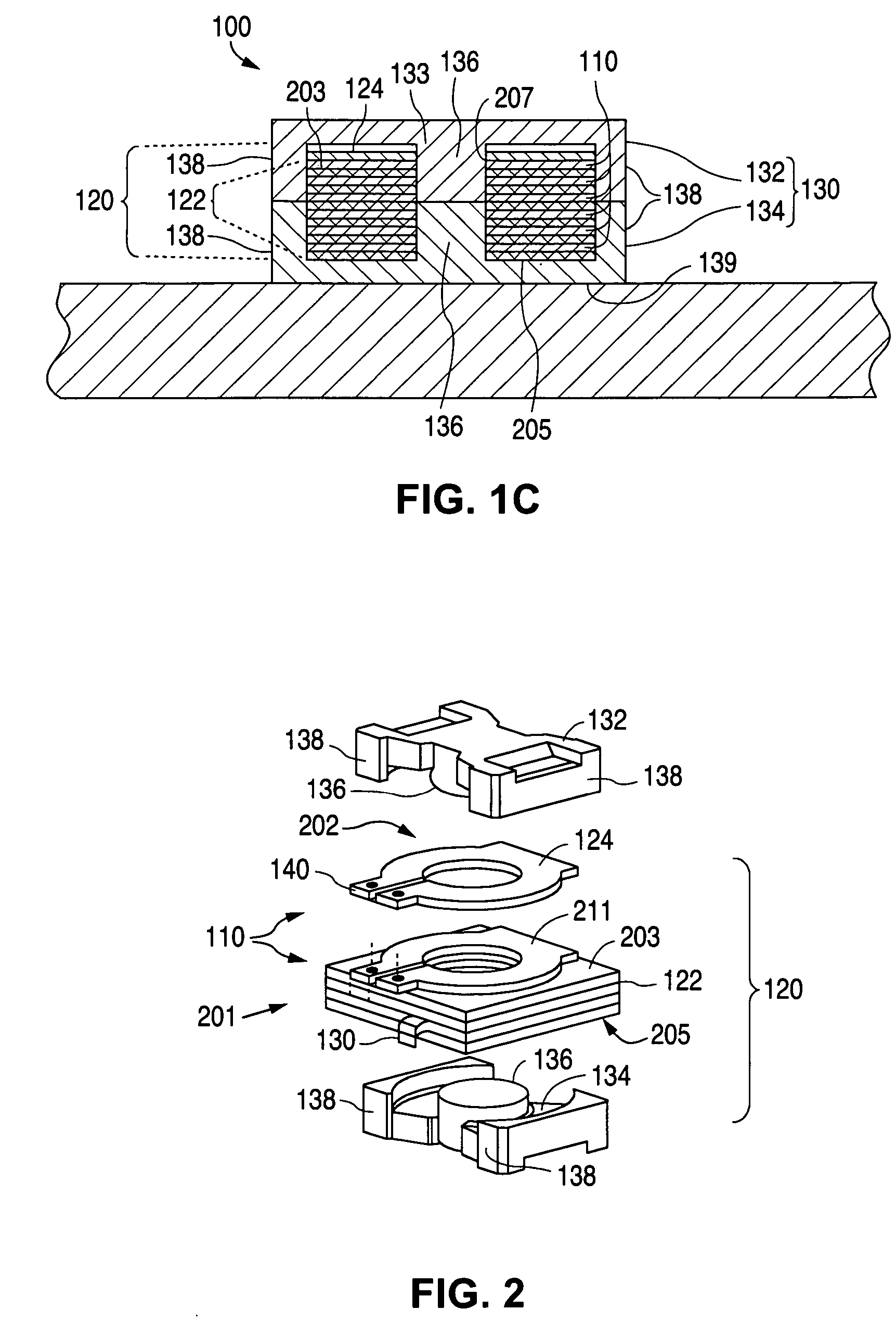
[0040] To facilitate its description, the invention is described below in terms of inductors or transformers having windings whose turns are formed by traces, each of which are patterned on the surface of a different insulating layer of a multi-layer PCB, and wherein at least one winding turn includes a conductive layer that is not a PCB trace. In general, the present invention provides an electromagnetic component that is formed using a multi-layer PCB, where the component can comprise a transformer, or the like.

[0041] The inventive PCB winding includes a plurality of conductive layers or traces wherein each conductive trace is formed on an insulating layer of said PCB and is positioned with respect to the other conductive traces such that the conductive traces form a stack. An additional conductive layer, such as a metal foil, is attached to an outer surface of the PCB. The additional conductive layer can form a separate loop of the winding, or can be connected in parallel with a...


PUM


Abstract

The present invention provides a transformer formed from adjacent conducting layers of a multi-layer PCB and at least one additional conducting layer in contact with the PCB. The inventive transformer includes one or more winding turns of a first winding formed by connecting the multiple layers of the multi-layer PCB with conductive vias and one or more winding turns of a second winding formed by connecting one or more other layers of the multi-layer PCB. The additional conducting layer or layers is connected to respective selected one or more of said conducting layers of said PCB. In one embodiment, an additional conducting layer is soldered to a top conducting layer of the PCB, effectively increasing the cross-sectional area of the top winding layer. In another embodiment, an additional conducting layer is separated from a conducting PCB layer formed on the surface thereof by a layer of insulation, permitting the additional conducting layer to form a separate winding turn. The inventive transformer can be surface mounted to a PCB, and can be used in other electromagnetic devices. The windings thus constructed are capable of accepting larger currents with lower resulting temperature increases than windings formed only from PCBs, and are less expensive to manufacture than PCB-only windings.

Description

FIELD OF THE INVENTION [0001] The present invention relates to electromagnetic components for electric circuits, such as inductors and transformers and, in particular, to the formation of one or more winding turns of a transformer using a multi-layer printed circuit board. BACKGROUND OF THE INVENTION [0002] Electromagnetic components such as inductors and transformers have traditionally been constructed by winding one or more conductors about a cylindrical or torroidal core. This method of construction requires that a conductor, such as a wire, be wrapped around the outer surface of the core. The resulting components are expensive and time consuming to manufacture, and do not readily lend themselves to miniaturization or automated assembly. [0003] More recently, electromagnetic components have been constructed using printed circuit board (PCB) manufacturing techniques, where windings and individual winding turns are formed from one or more conducting layers patterned on the surface ...

Claims


Application Information

Patent Timeline
IPC IPC(8): H01F17/00H01F17/04H01F27/06H01F27/28
CPCH01F17/0013H01F27/2804H01F17/043
Inventor CHIANG, MAN-HOCHUNG-HANG, FRANCOIS LAI
Owner ASTEC INT LTD
Why Eureka
Try Eureka