Multiple-select multiplexer circuit, semiconductor memory device including a multiplexer circuit and method of testing the semiconductor memory device

a multiplexer circuit and multiplexer technology, applied in pulse manipulation, pulse technique, instruments, etc., can solve the problems of wired or logic using the tri-state buffer, large current consumption, and long cycle tim

Inactive Publication Date: 2005-09-29
KK TOSHIBA
View PDF5 Cites 6 Cited by
  • Summary
  • Abstract
  • Description
  • Claims
  • Application Information

AI Technical Summary

Benefits of technology

[0022] a first drive timing control circuit supplied with an output signal of the first unmatch detection circuit, the data signal, the segment select signal and the second control signal, outputting the select signal and an output signal of the segment select circuit in accordance with the output signal of the first unmatch detection circuit when the second control signal is in a non-active state while keeping an old output state when the second control signal is in an active state; and
[0023] a first tri-state buffer receiving an output signal of the first drive timing control circuit, driving each of the common lines according to a state of the data signal in synchronous with the second control signal, and keeping a state for an active period of the second control signal while the output becomes high impedance state when the second control signal becomes a non-active state;

Problems solved by technology

However, pre-charge and discharge operations are repeated in one-time logic operation; for this reason, current consumption becomes large, and also, cycle time becomes long.
On the other hand, the wired OR logic using the tri-state buffer has the problem described below.
As a result, there is a possibility that damage is given to lines and semiconductor elements.
In particular, if the foregoing accident happens in a burn-in operation such that high power supply voltage is applied, it is getting more and more serious.
However, the technique described in the Publication 2-235435 does not solve the problem peculiar to multiplexers although it enhances the rise or fall speed of the output waveform.

Method used


Image

  • Multiple-select multiplexer circuit, semiconductor memory device including a multiplexer circuit and method of testing the semiconductor memory device
  • Multiple-select multiplexer circuit, semiconductor memory device including a multiplexer circuit and method of testing the semiconductor memory device
  • Multiple-select multiplexer circuit, semiconductor memory device including a multiplexer circuit and method of testing the semiconductor memory device

Examples


first embodiment

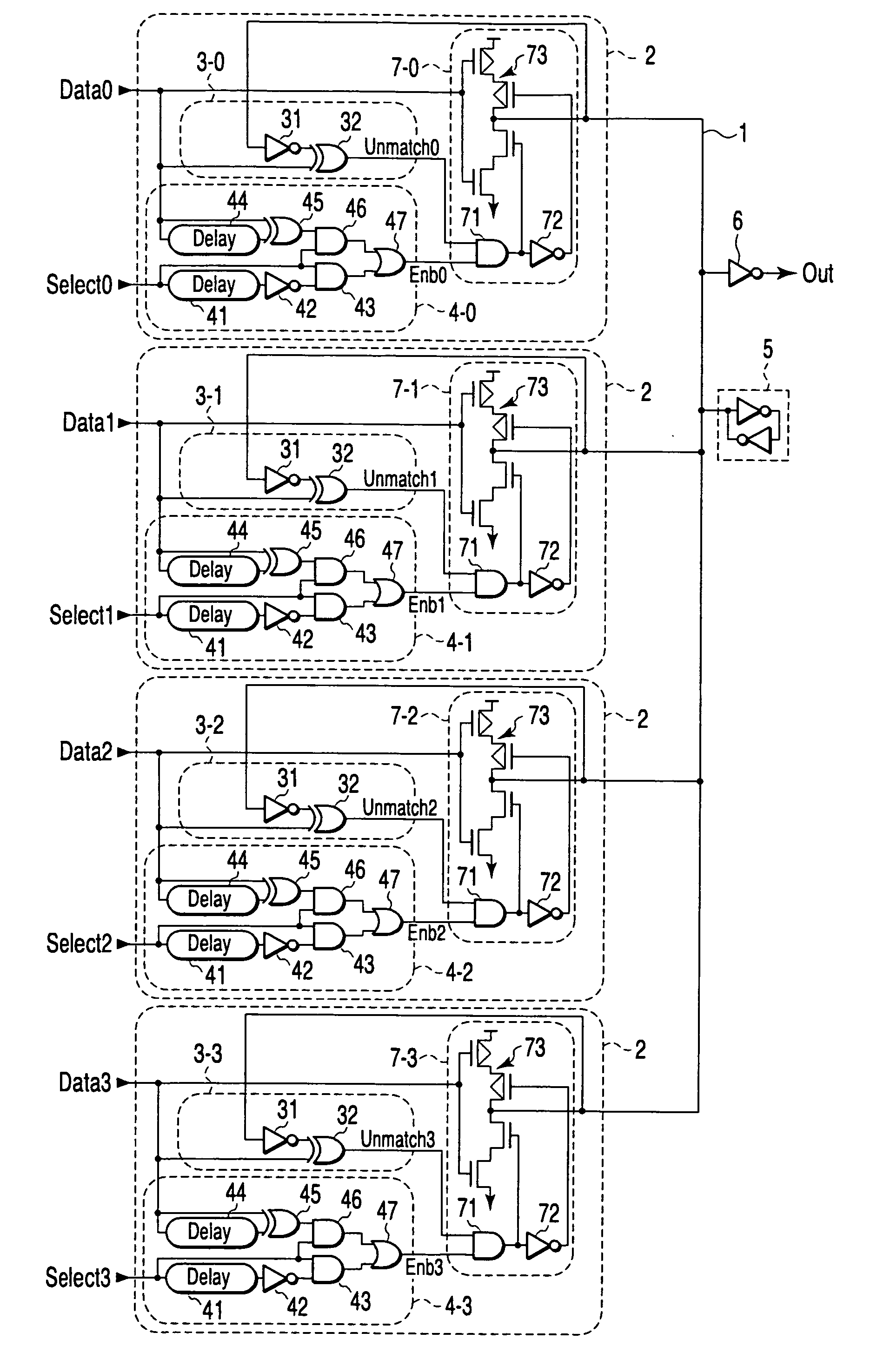
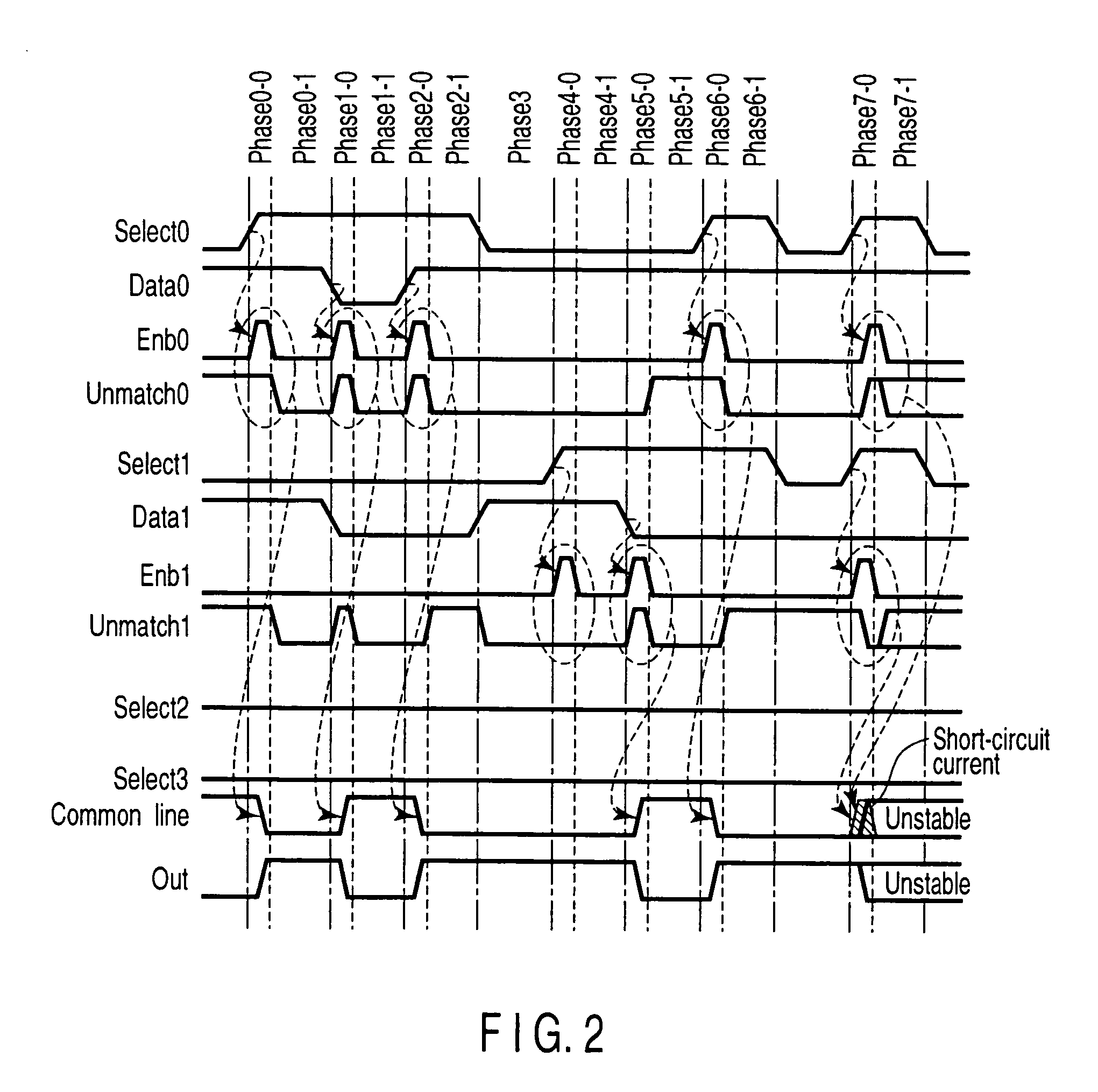
[0038]FIG. 1 is a circuit diagram showing the configuration of an asynchronous multiplexer circuit according to the present invention. The multiplexer circuit is built in an LSI. The multiplexer circuit has several, that is, four basic unit circuits 2, common line 1, state holding circuit 5 and output buffer 6. The common line 1 is commonly connected with each output terminal of the basic unit circuit 2, which makes wired OR connection. The state holding circuit 5 is connected to the common line 1, and has minute output current for holding a signal in the common line 1. The output buffer 6 receives the signal of the common line 1 to generate an output signal (out).

[0039] The basic unit circuits 2 each includes unmatch detection circuit 3-i (i=0˜3), drive timing control circuit 4-i (i=0˜3), and synchronous tri-state buffer 7-i (i=0˜3).

[0040] The unmatch detection circuit 3-i (i=0˜3) detects unmatch of a data signal datai (i=0˜3) with the signal state of the common line 1. The drive ...

second embodiment

[0071] The second embodiment shows the asynchronous multiplexer circuit, which carries out specific timing control. The specification of the select signal selecti may be variously modified. The any number of the basic unit circuits 2 may be provided so long as it is more than two.

[0072] In the first and second embodiments, the relation between the potential and state of the common line 1 is negative logic. The configuration of internal logic circuits is changed, and thereby, positive logic may be employed. Likewise, the circuit configuration may be variously modified in drive timing control circuit 4-i, tri-state buffer 7-i, state holding circuit 5 and output buffer 6.

[0073]

third embodiment

[0074]FIG. 5 is a circuit diagram showing the configuration of a synchronous multiplexer circuit according to the present invention. The multiplexer circuit is composed of four basic unit circuits 2, common line 1, state holding circuit 5 and output buffer 6. The basic unit circuits 2 input a signal datai and a select signal selecti. The common line 1 is commonly connected with each output terminal of the basic unit circuits 2. The state holding circuit 5 holds the state of the common line 1. The output buffer 6 receives a signal of the common line 1 to generate an output signal out.

[0075] The basic unit circuits 2 each commonly input a clock signal clock for controlling operation timing. The basic unit circuits 2 each includes unmatch detection circuit 3-i, drive timing control circuit 4-i, and synchronous tri-state buffer 7-i. The basic unit circuits 2 each input the signal datai and the select signal selecti. Then, the basic unit circuits 2 each output a state of the signal datai...


PUM


Abstract

A multiplexer circuit is composed of several basic unit circuits, which are each supplied with a data signal and select signal. Each output terminal of several basic unit circuits is connected to a common line. Each basic unit circuit is composed of an unmatch detection circuit detecting an unmatch state of the common line and the data signal, a control circuit controlling drive timing of the common line when receiving a state transition of the select signal, and a tri-state buffer driving the common line according to a state of the data signal when an output of the unmatch detection circuit and an output of the control circuit are both in an active state while holds high impedance state when the state other than above is given.

Description

CROSS-REFERENCE TO RELATED APPLICATIONS [0001] This application is based upon and claims the benefit of priority from prior Japanese Patent Application No. 2004-087166, filed Mar. 24, 2004, the entire contents of which are incorporated herein by reference. BACKGROUND OF THE INVENTION [0002] 1. Field of the Invention [0003] The present invention relates to a multiple-select multiplexer circuit, a semiconductor memory device including a multiplexer circuit, and a memory segment parallel test method of the semiconductor memory device. [0004] 2. Description of the Related Art [0005] For example, wired OR logic is employed to form a multiplexer circuit, which selects one data line from several data lines provided in a semiconductor memory. In the wired OR logic, several drivers makes cascade connection with respect to one line (conducting path, interconnection). Two kinds, that is, domino circuit and tri-state buffer have been known as the driver. [0006] In general, the wired OR logic us...

Claims


Application Information

Patent Timeline
Patent Type & Authority Applications(United States)
IPC IPC(8): G01R31/28G11C5/00G11C7/10G11C11/401G11C29/00G11C29/06G11C29/34H03K5/00H03K17/00H03K17/16
CPCG11C7/1012G11C7/1051G11C11/401G11C2029/2602G11C29/1201G11C29/26G11C29/40G11C29/06
Inventor NAMEKAWA, TOSHIMASA
Owner KK TOSHIBA
Why Eureka
Try Eureka