Arsenic dopants for pulling of silicon single crystal, process for producing thereof and process for producing silicon single crystal using thereof

a technology of arsenic dopants and silicon single crystals, which is applied in the direction of polycrystalline material growth, chemistry apparatus and processes, crystal growth processes, etc., can solve the problems of difficult control of the operation of adding the dopant to a high concentration, limited use of phosphorus for and inability to reduce the resistivity of silicon single crystals. , to achieve the effect of reducing the resistivity of silicon single crystals

Inactive Publication Date: 2005-09-29
TOSHIBA CERAMICS CO
View PDF6 Cites 6 Cited by
  • Summary
  • Abstract
  • Description
  • Claims
  • Application Information

AI Technical Summary

Benefits of technology

[0013] According to embodiments of the present invention, it is an object of the present invention to provide an arsenic dopant to be used for pulling of silicon single crystal that can efficiently dope silicon single crystal with arsenic to remarkably reduce the resistivity of silicon single crystal and the intra-planar resistance of silicon single crystal in radial directions, a process for producing such an arsenic dopant and a process for producing silicon single crystal, using such an arsenic dopant.

Problems solved by technology

Thus, the use of a large amount of phosphorus for reducing the resistivity of silicon single crystal is inevitably limited.
Thus, the use of antimony for reducing the resistivity of silicon single crystal is also inevitably limited.
Therefore, it is difficult to control the operation of adding the dopant to a high concentration.
Additionally, when arsenic is used alone as dopant, it can give rise to highly toxic arsenic oxide (III) (As2O3) in air, which is very hazardous to the attending workers and can highly possibly harm the health of the workers.
However, a coated arsenic dopant as described in Patent Document 1 has a drawback that the arsenic atoms can be exposed to air to give off highly toxic arsenic oxide (III) (As2O3), which is very hazardous, once the coat is destroyed, if partly.
Additionally, when the dopant is dissolved into raw material silicon melt, the coat of the dopant can easily dissolve and become lost while it is floating on the surface of the melt.
Thus, it is difficult to sufficiently reduce the resistivity of silicon single crystal.
While, on the other hand, an arsenic dopant as described in Patent Document 2 is not accompanied by the risk of giving off arsenic oxide (III), it contains silicon to a large extent and hence it is difficult to sufficiently reduce the resistivity of silicon single crystal by using such an arsenic dopant.

Method used


Image

  • Arsenic dopants for pulling of silicon single crystal, process for producing thereof and process for producing silicon single crystal using thereof
  • Arsenic dopants for pulling of silicon single crystal, process for producing thereof and process for producing silicon single crystal using thereof
  • Arsenic dopants for pulling of silicon single crystal, process for producing thereof and process for producing silicon single crystal using thereof

Examples


examples

[0034] Powdery silicon (atomic weight: 28.09) was added to 100 g of granular arsenic (atomic weight: 79.92) with a grain diameter of 2 mm to molar ratios of 0% (Comparative Example 1), 25% (9.4 g: Comparative Example 2), 35% (13.1 g: Example 1), 45% (16.9 g: Example 2), 50% (18.75 g: Example 3), 55% (20.6 g: Example 4), 60% (22.5 g: Comparative Example 3) and the mixtures were held in vacuum in a hermetically sealed condition in respective quartz tubes and baked at 900° C. for seven days for a sintering reaction. Thus, As dopants of seven different types for pulling of silicon single crystal were obtained as a result of a sintering reaction.

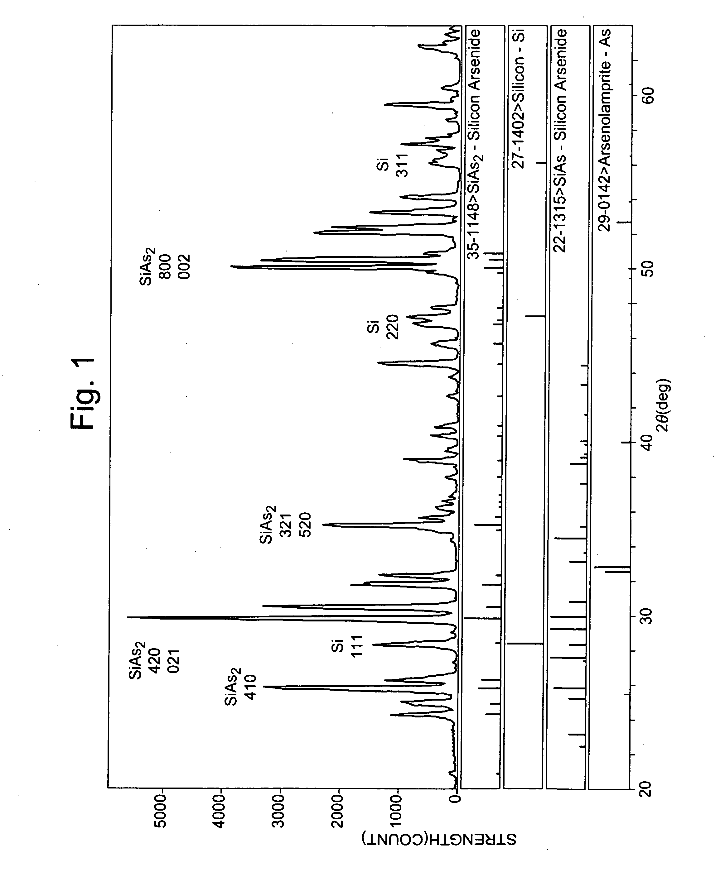
[0035] The obtained As dopant for pulling of silicon single crystal of Example 3 was observed by means of an X-ray diffractometer (XRD) to identify the produced compound. As a result, a compound of SiAs2 and silicon, which is the sintering residue, were observed as shown in FIG. 1.

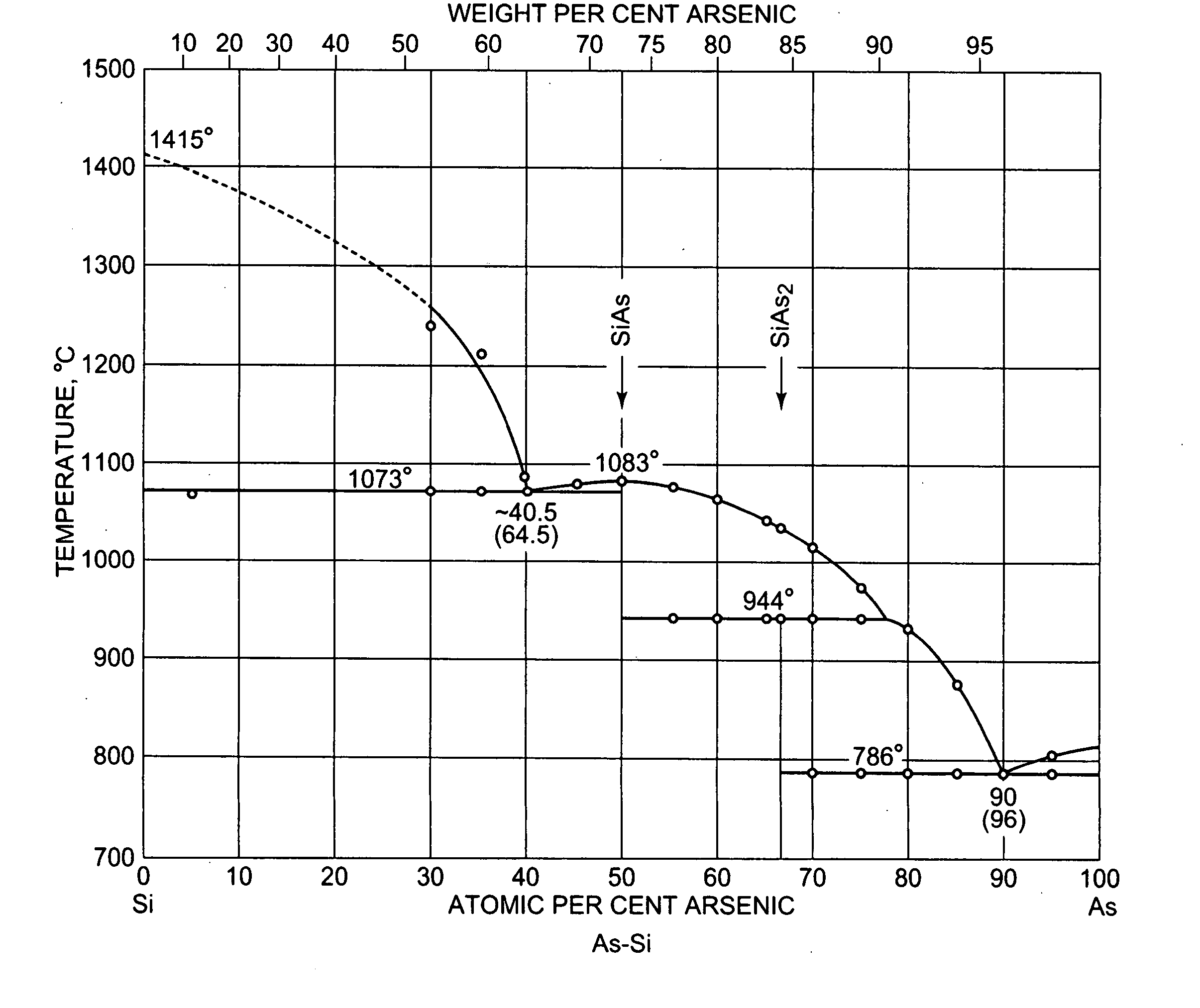
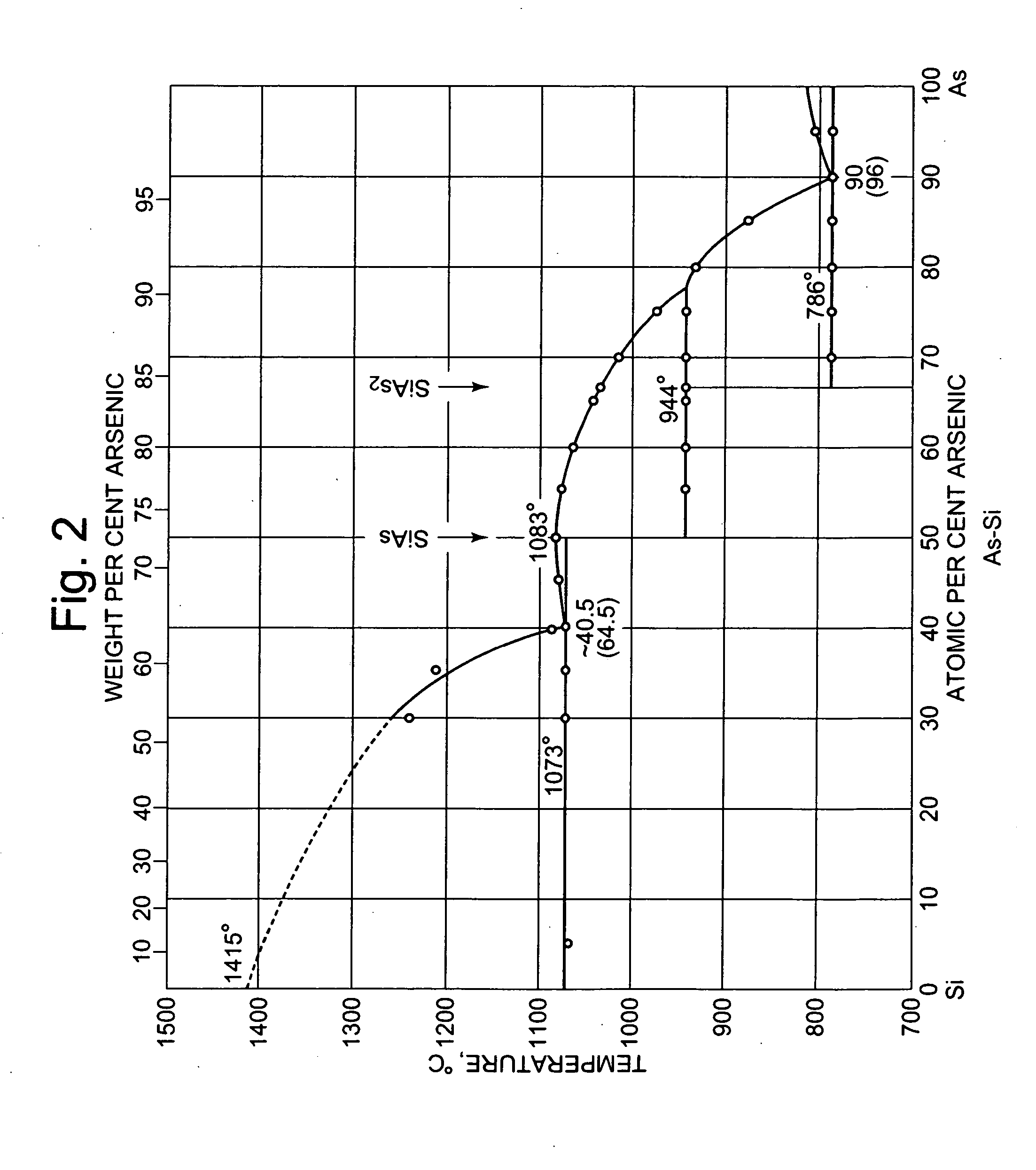
[0036] While there are two compounds of silicon arsenide includi...


PUM

PropertyMeasurementUnit
temperatureaaaaaaaaaa
melting pointaaaaaaaaaa

Abstract

Silicon single crystal is pulled by the Czochralski method, using an As dopant comprising a mixed sintered compact of arsenic and silicon, the molar ratio of silicon being not smaller than 35% and not greater than 55% relative to arsenic.

Description

CROSS-REFERENCE TO RELATED APPLICATIONS [0001] This application is based upon and claims the benefit of priority from the prior Japanese Patent Application No. 2004-96208, filed on Mar. 29, 2004 and No. 2005-007335, filed on Jan. 14, 2005, the entire contents of which are incorporated herein by reference. BACKGROUND OF THE INVENTION [0002] 1. Field of the Invention [0003] The present invention relates to an arsenic dopant for pulling of silicon single crystal to be used for doping when growing silicon single crystal by means of the Czochralski method, a process for producing thereof and a process for producing silicon single crystal using thereof. [0004] 2. Description of the Related Art [0005] When producing silicon single crystal by means of the Czochralski method, the resistivity is controlled to a desired level according to the specification and the object of the production. The resistivity (specific resistance) is controlled by adding a dopant such as phosphorus (P), antimony (...

Claims


Application Information

Patent Timeline
Patent Type & Authority Applications(United States)
IPC IPC(8): C30B29/06C30B1/02C30B15/04H01L21/26H01L21/302H01L21/42H01L21/461
CPCC30B29/06C30B15/04
Inventor KASHIMA, KAZUHIKO
Owner TOSHIBA CERAMICS CO
Why Eureka
Try Eureka