Printed circuit board and manufacturing method thereof

a technology of printed circuit boards and manufacturing methods, applied in the direction of printed circuit non-printed electric components association, fixed capacitors, liquid electrolytic capacitors, etc., can solve the problems of signal delay, equipment malfunction, and insufficient thickness, and achieve high-reliability connection, simple structure, and preferable thinning

Inactive Publication Date: 2005-10-06
TOKIN CORP
View PDF2 Cites 18 Cited by
  • Summary
  • Abstract
  • Description
  • Claims
  • Application Information

AI Technical Summary

Benefits of technology

[0017] Preferably, the electrodes of the buried capacitor device are connected to the conductor pattern of the upper layer by the via holes. When the conductor pattern of the upper layer is an outer layer of the printed circuit board, the surfaces of the via holes filled by electrolytic copper plating or conductive paste are flat. Since their surfaces are flat, no voids are caused in solder used for connection to the parts mounted on the surface of the printed circuit board, enabling high-reliability connection.
[0018] According to of the present invention, a capacitor device has a dielectric layer formed on at least one side of a planar metal substrate, an ano

Problems solved by technology

The increased number of leads of mounted parts, smaller pitch, increased wiring resistance with a higher multi-layer printed circuit board due to a growing number of mounted parts and finer lines, signal delay due to cross talk noise, heat generation, and malfunc

Method used


Image

  • Printed circuit board and manufacturing method thereof
  • Printed circuit board and manufacturing method thereof
  • Printed circuit board and manufacturing method thereof

Examples


Embodiment Construction

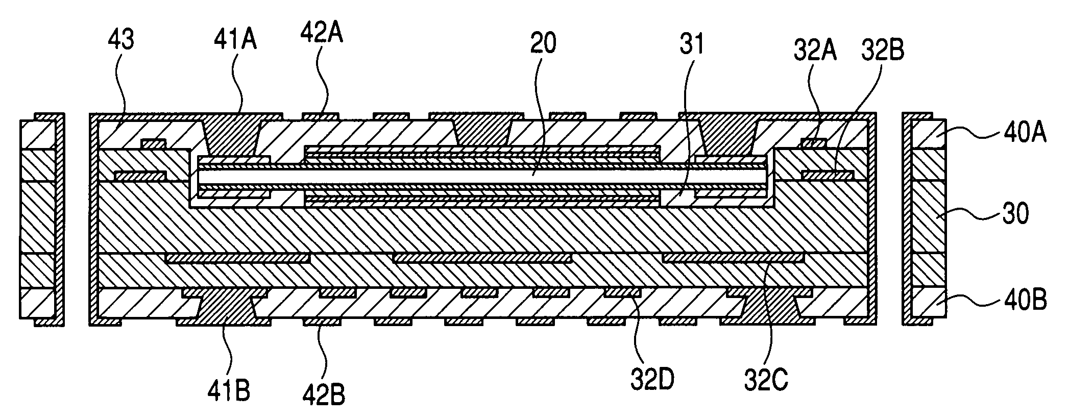
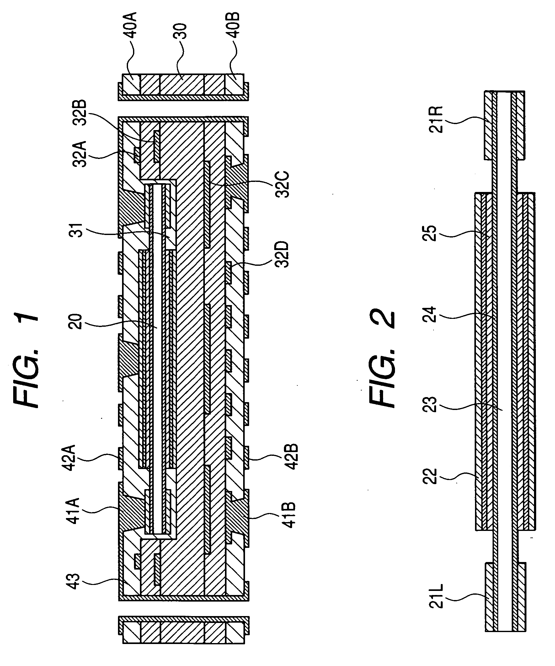
[0030] The structure of a printed circuit board according to an embodiment of the present invention will be described below with reference to the drawings. FIG. 1 shows the cross section of a printed circuit board.

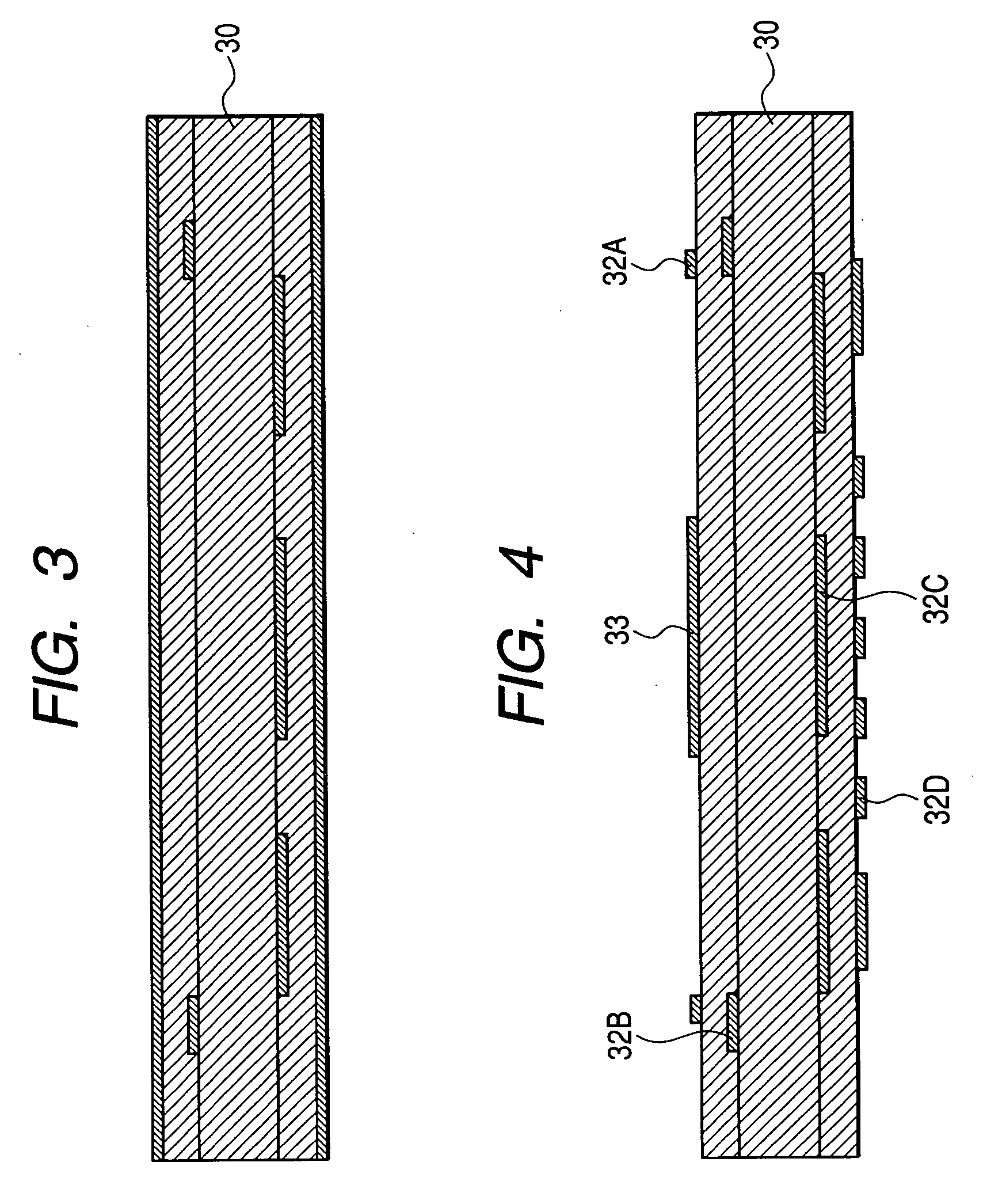
[0031] A printed circuit board has an unpackaged capacitor device 20, a core substrate 30 housing the capacitor device, and buildup layers 40A and 40B. The core substrate 30 has a recess part 31 housing the unpackaged capacitor device 20 and plural conductor layers 32A, 32B, 32C, and 32D on the surfaces and inside thereof. The buildup layer 40A is formed with via holes 41A and a conductor circuit 42. The conductor circuit 32A on the surface of the core layer, the unpackaged capacitor device 20, and a conductor circuit 42A of the buildup layer are connected by via holes 41A. The buildup layer 40B is formed with via holes 41B and a conductor circuit 42B. The conductor circuit 32D on the surface of the core layer is connected to the conductor circuit 42B of the buildup layer...


PUM

PropertyMeasurementUnit
Thicknessaaaaaaaaaa
Thicknessaaaaaaaaaa
Thicknessaaaaaaaaaa

Abstract

A printed circuit board which is thin and incorporates a large-capacitance capacitor function and a manufacturing method thereof. In one embodiment, the printed circuit board manufacturing method includes forming inner layer conductor circuits on a core substrate; forming a recess part on the core substrate; housing, in a recess part, a planar capacitor device that is not resin molded and has electrodes on the surfaces on a shared side; interposing the same between insulator resin and conductor metal foil to heat pressurize the same for forming a multi-layer plate; forming via holes for electrically connecting an outer layer conductor circuit to the electrodes of the capacitor device; forming a conductor layer on them; and forming the outer layer conductor circuits on the surfaces of the multi-layer plate.

Description

BACKGROUND OF THE INVENTION [0001] 1. Field of the Invention [0002] The present invention relates to a printed circuit board and a manufacturing method thereof. More specifically, the present invention relates to a multi-layer printed circuit board incorporating a capacitor function and a manufacturing method thereof. [0003] 2. Description of Related Art [0004] With the higher performance of electronic equipment, the number of parts mounted on a printed circuit board is being increased. Due to the miniaturization of electronic equipment, the size of the printed circuit board is required to be further reduced. The area on which the parts can be mounted is being made smaller. [0005] With reduction of the parts in size, the density of surface mounting is becoming higher due to microfabrication of the conductor pattern of the printed circuit board. [0006] The increased number of leads of mounted parts, smaller pitch, increased wiring resistance with a higher multi-layer printed circuit ...

Claims


Application Information

Patent Timeline
IPC IPC(8): H01G2/06H01G4/00H05K1/00H05K1/02H05K1/16H05K1/18H05K3/46
CPCH05K1/0231H05K1/162H05K1/185Y10T29/49155H05K2201/0329H05K2203/0315Y10T29/49165H05K3/4644H05K1/183A01G9/02E02B3/14E02D17/205
Inventor NOGUCHI, SETSUOTAKAHASHI, KOHTAROHMATSUNAGA, EIJISAIKI, YOSHIHIKOARAI, SATOSHITOITA, SADAMU
Owner TOKIN CORP
Why Eureka
Try Eureka