Infrared sensor

Inactive Publication Date: 2005-10-06
JAPAN AVIATION ELECTRONICS IND LTD
View PDF4 Cites 17 Cited by
  • Summary
  • Abstract
  • Description
  • Claims
  • Application Information

AI Technical Summary

Benefits of technology

[0013] With the above configuration of the infrared sensor according to the present invention, the incident infrared light can be focused to a spot size smaller than its wavelength and guided in parallel to the substrate surface to thereby increase the quantity of infrared light incident on the infrared absorbing part, permitting implementation of high sensitivity and fast responsivity.

Problems solved by technology

Generally speaking, the quantum sensor calls for cooling, and hence it is hard to get small in size and is expensive.
On the other hand, despite its inferiority in performance, for example, in sensitivity and responsivity, to the quantum sensor, the thermal sensor need not be cooled and can be made smaller in size and lower in price, and hence it is now widely used for measuring slow changes in temperature (a clinical thermometer, for instance) or for sensing a slowly moving object (an intrusion sensor, for instance).
However, some problems need to be solved to provide compatibility between the demand for further increase in the quantity of infrared absorption per unit area and the demand for cost reduction by downsizing the sensor and simplification of its manufacturing process.
However, the reduction of the focused spot size calls for separating the lens and the infrared absorbing part from each other, inevitably making the sensor structure bulky.
Even if they are sufficiently spaced apart, the focused spot size cannot be made smaller than the infrared wavelength.
Besides, since the support frame with the lenses and the substrate with

Method used


Image

  • Infrared sensor
  • Infrared sensor
  • Infrared sensor

Examples


embodiment 1

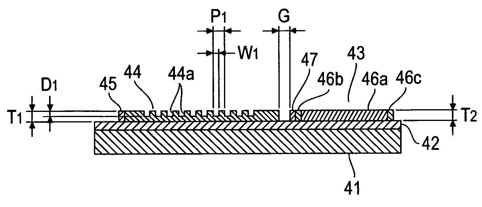
[0036]FIGS. 3A and 3B illustrate a first embodiment of the infrared sensor according to the present invention. In this embodiment a silicon (Si) substrate 41 is coated over the entire surface area thereof with an SiO2 film 42 as an electrical and heat insulation film, on which there are disposed side by side an infrared detector 43 for converting infrared light to an electric signal and an optical element 44 for guiding the infrared light to the infrared detector 43.

[0037] The optical element 44 having an array of materials of different refractive indexes is, in this embodiment, a planar optical waveguide having a diffraction grating on the top, and the waveguide is formed of silicon. Straight grooves 44a forming the diffraction grating are formed with a pitch P1=8 μm and each groove has a width W1=4 μm and a depth D1=0.5 μm, and the thickness T1 of the optical element 44 is 2 μm.

[0038] The optical element 44 is formed by: forming a silicon film all over the surface area of the Si...

embodiment 2

[0044]FIGS. 4A and 4B illustrate a second embodiment of the present invention, in which the substrate 41 covered with the SiO2 film 42 of the infrared sensor shown in FIGS. 3A and 3B is substituted with a flexible plastics film 51, on which the infrared detector 43 and the optical element 44 are formed as is the case with the embodiment shown in FIGS. 3A and 3B. In this embodiment the infrared sensor is flexible.

[0045] A check was made on the durability of the infrared sensor to being of the plastics film 51 (on the degree of bending to which the function of the infrared sensor could be maintained), and it was found that the durability of the infrared sensor depends greatly on the thickness of the optical element 44. The reason for this is given below. In the infrared sensor of this embodiment the optical element 44, which occupies a large area, is formed of a semiconductor material such as silicon or dielectric material such as glass transparent to infrared rays, and since these m...

embodiment 3

[0046]FIGS. 5A and 5B illustrate a third embodiment of the present invention, in which there is cut in the substrate 41 a deep groove 52 corresponding to the gap G between the optical element 44 and the infrared detector 43. The deep groove 52 is formed by etching, and it has a width W4 of 10 μm and a depth D4 of 100 μm.

[0047] The provision of the deep groove 52 suppresses the conduction of heat converted by the infrared absorption layer 47 to the optical element 44 and the substrate 41 to provide increased thermal insulation property of the infrared absorption layer 47 to further increase its temperature-rise ratio, permitting implementation of higher sensitivity and faster responsivity. In the manufacture of the infrared sensor according to this embodiment, the infrared detector 43 and the optical element 44 are formed oppositely across the deep groove 52 preformed in the substrate 41.


PUM


Abstract

An infrared sensor which is provided with an infrared detector 43 for converting infrared light to an electric signal and an optical element 44 for guiding the infrared light to the infrared detector 43, and in which the optical element 44 is a planar optical waveguide provided with a diffraction grating and is formed on a substrate 41 side by side with the infrared detector 43. The infrared light incident on the optical element 44 from a direction vertical to the substrate surface is deflected and guided by the optical element 44 in parallel to the substrate surface for incidence on the infrared detector 43. The infrared sensor is small in size, highly sensitive, fast in responsivity, and easy to manufacture.

Description

BACKGROUND OF THE INVENTION [0001] The present invention relates generally to an infrared sensor provided with an infrared detector and an optical element for guiding thereto infrared light and, more particularly, to a small, low-profile infrared sensor that achieves high infrared detection sensitivity and high-speed responsivity by increasing the quantity of infrared light incident on the infrared detector per unit area through use of an optical element capable of controlling the direction of travel of infrared light and focusing it to a spot size smaller than its wavelength. [0002] Infrared sensors for converting infrared light from a heat source to an electric signal are roughly divided into a thermal and a quantum sensor. The thermal sensor is one that induces a temperature change in a sensor material by converting infrared light to heat through an infrared absorption layer or the like and detects a change in electromotive force, distribution of electric charge, or resistance va...

Claims


Application Information

Patent Timeline
IPC IPC(8): G01J1/04G01J1/02G01J5/02G01J5/08G01J5/12G01J5/14H01L27/14H01L35/32
CPCG01J5/02G01J5/022G01J5/024G01J5/08G01J5/12G01J5/0806G01J5/0818G01J5/0853G01J5/0884G01J5/0803
Inventor SUZUKI, AKIKOSATO, AKINOBUBOURELLE, EMMANUEL
Owner JAPAN AVIATION ELECTRONICS IND LTD
Why Eureka
Try Eureka