Display device

a technology of a display device and a light emitting element, which is applied in the direction of electroluminescent light sources, identification means, instruments, etc., can solve the problems of reducing luminance or non-light emission, reducing long-time reliability, and easy deterioration of light emitting elements using organic materials, so as to prevent deterioration of light emitting elements in light emitting devices, the effect of low water permeability

Active Publication Date: 2005-10-06
SEMICON ENERGY LAB CO LTD
View PDF39 Cites 145 Cited by
  • Summary
  • Abstract
  • Description
  • Claims
  • Application Information

AI Technical Summary

Benefits of technology

[0012] Yet another aspect of a light emitting device according to the invention will be described below. The light emitting device of the invention having a light emitting element comprising a light emitting layer formed between a first electrode and second electrode, and formed in the pixel portion. The light emitting device further includes a pixel portion formed of the light emitting element, and a thin film transistor. The second electrode covers the pixel portion. A first interlayer insulating film formed to cover the thin film transistor. An opening former so as to provide around at least a part of a circumference of the pixel portion and formed in the first interlayer insulating film. The opening passes through the first interlayer insulating film in the thickness direction. And the side and bottom faces of the opening are covered with an insulating film with a low water permeability. A second interlayer insulating film formed over the first interlayer insulating film, and the second interlayer insulating formed in contact with the insulating film and covering the first electrode. The first electrode is formed on the second interlayer insulating film and a partition wall is formed to cover the edge of the first electrode. The edge of the partition wall is in contact with the film with the low water permeability covering the side wall and the bottom face of the opening the partition wall formed in contact with the insulating film and covering the second electrode. The light emitting device of the invention having the above structure can overcome the above-mentioned problem.
[0013] According to the foregoing structures, the ingress of moisture into the light emitting layer can be reduced. Also, deterioration of light emitting element in the light emitting device can be prevented. Furthermore, the reliability of the light emitting device can be improved.

Problems solved by technology

The light emitting element using an organic material is easily deteriorated due to moisture (water) and has a drawback in which long-time reliability is difficultly obtained.
The light emitting element deteriorated by water results in decrease in luminance or non-light emission.
It has been thought that these defects might cause dark spots (black spots) or shrinkage (which is a deterioration in luminance caused from the end of a light emitting device) in a light emitting device.
However, the above measures have not overcome the above-mentioned problems and an adequate level of reliability has not been obtained.

Method used


Image

  • Display device
  • Display device
  • Display device

Examples


embodiment mode 1

[Embodiment Mode 1]

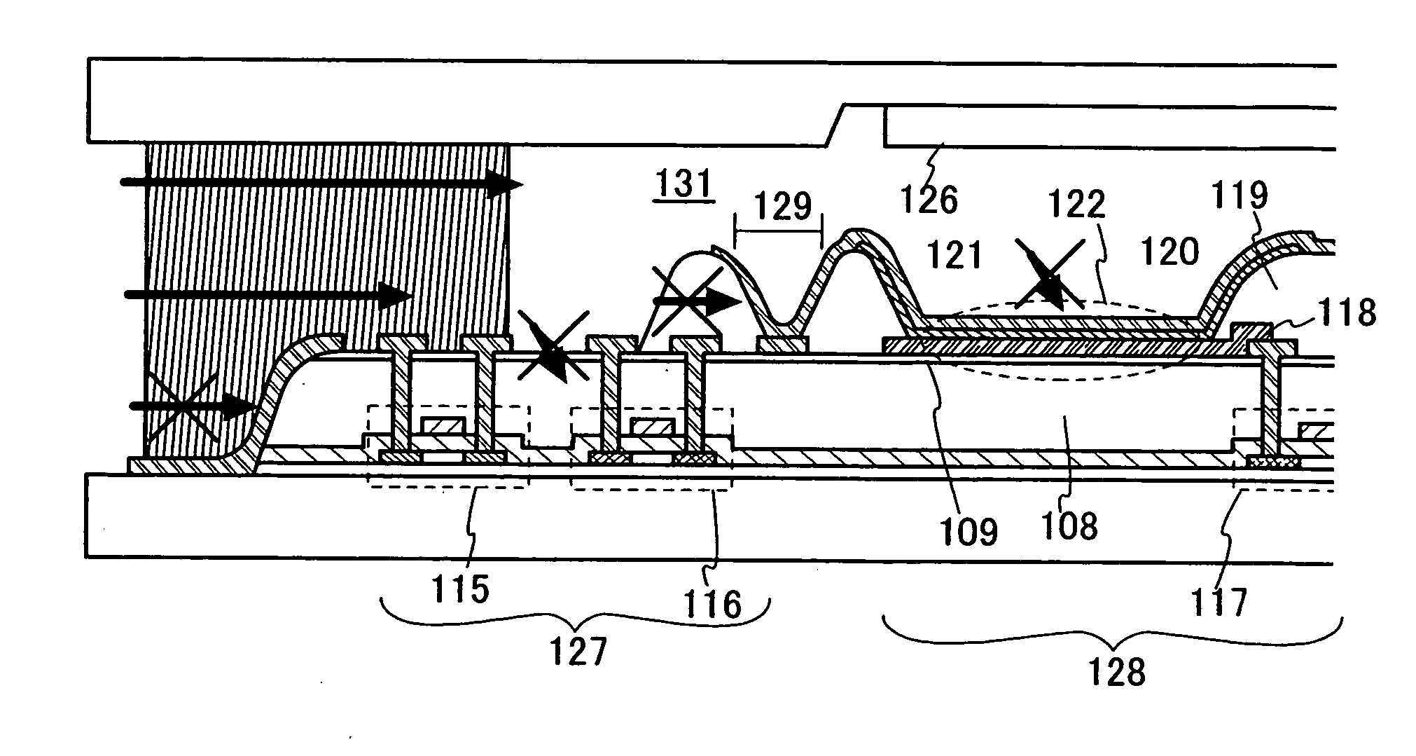
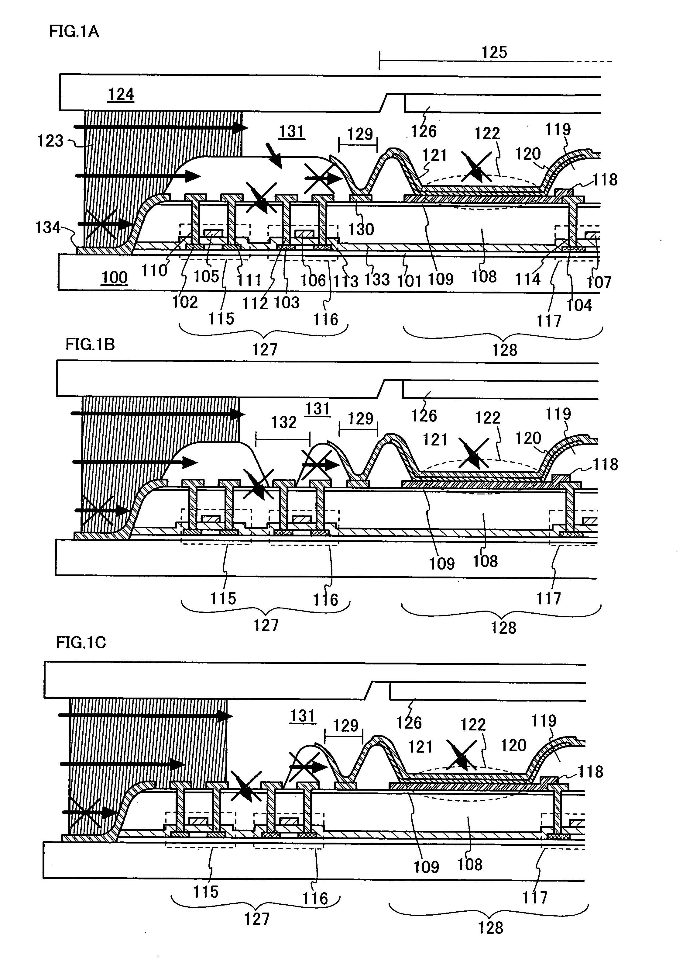
[0042]FIGS. 1A to 1C are cross sectional views of the light emitting device according to the invention. A base insulating film 101 is formed on a substrate 100. Semiconductor layers 102 to 104 are formed thereon. The base insulating film 101 and the semiconductor layers 102 to 104 are covered with a gate insulating film 133. Gate electrodes 105 to 107 are formed on the gate insulating film 133 while partly overlapping with the semiconductor layers 102 to 104. The gate insulating film 133 and the gate electrodes 105 to 107 are covered with an interlayer insulating film 108. An insulating film 109 is formed on the interlayer insulating film 108.

[0043] The substrate 100 serves to support thin film transistors and a light emitting element. The base insulating film 101 is formed to prevent a substance that adversely affects the thin film transistors from dispersing through the substrate 100. If the adverse effect due to such the substance is of no matter, the base ins...

embodiment mode 2

[Embodiment Mode 2]

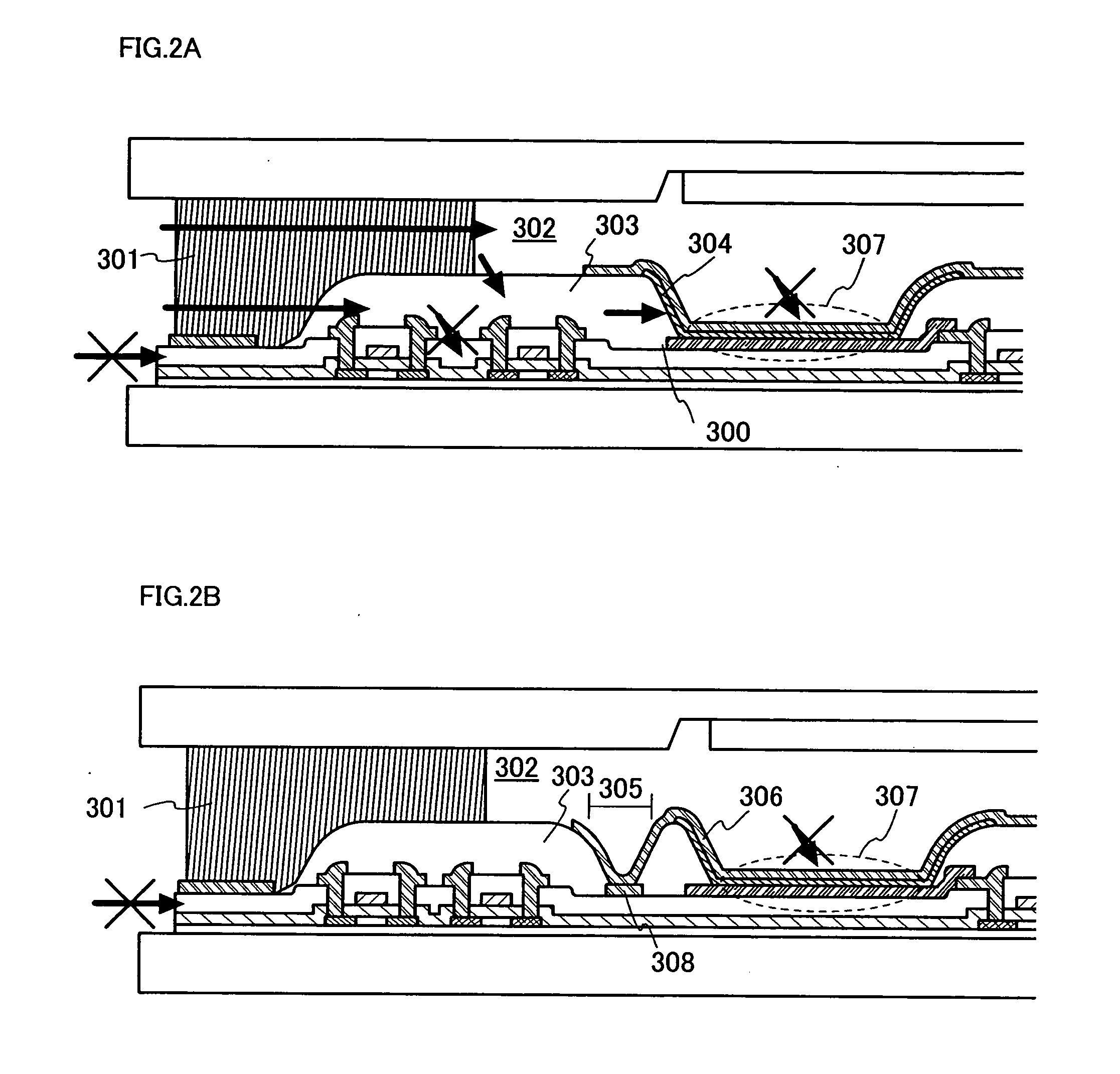
[0059] Another embodiment mode of the invention will be described in the present embodiment mode with reference to FIGS. 2A and 2B. Note that identical portions to those in FIGS. 1A to 1C may not be further explained.

[0060]FIG. 2B show examples in which an interlayer insulating film 300 is formed of a material such as silicon oxide, silicon nitride, silicon oxide containing nitrogen and silicon nitride containing oxygen. The interlayer insulating film 300 may include a single layer or lamination layer. Since these materials have a low water permeability and are hardly permeated with moisture if they are exposed to outside air, moisture hardly permeate through the interlayer insulating film 300 without covering the edge of the interlayer insulating film with a film 134 having a low water permeability as shown in FIG. 1A. In addition, the structure corresponding to the insulating film 109 as shown in FIG. 1A may not be provided. Note that other structure is same as...

embodiment mode 3

[Embodiment Mode 3]

[0065] Another embodiment mode of the present invention will be described with reference to FIG. 3. The portions identical with those in FIG. 1A to 1C may not be further explained.

[0066] In this embodiment mode, an example in which wirings 401 to 405 and a pixel electrode (a first electrode) 406 are located in different layers from one another will be explained. An insulating film 408 is formed on a first interlayer insulating film 407 in this embodiment mode. It is assumed that the first interlayer insulating film 407 is made from an organic insulating film such as acrylic and polyimide or an insulating film with a relatively high water permeability such as siloxane. Further, the insulating film 408 is made from a material with a low water permeability such as silicon nitride, silicon nitride containing oxygen, silicon oxide containing nitrogen and silicon oxide.

[0067] Note that one or more insulating films may be further provided between the first interlayer i...


PUM


Abstract

In a light emitting device using a light emitting element, the invention provides a sealing structure capable of preventing ingress of moisture from the outside and obtaining adequate reliability. The light emitting device has a light emitting element comprising a light emitting layer formed between a first electrode and a second electrode and a pixel portion comprising the light emitting element. The entire surface of the pixel portion is covered with the second electrode. An impermeable insulating film is formed in contact with the first electrode of the light emitting element. The edge of the first electrode and the impermeable insulating film are covered with a partition wall. An opening is formed along the circumference of the pixel portion in the partition wall. The opening passes through the partition wall in the thickness direction, and the side wall and the bottom face thereof are covered with the second electrode.

Description

BACKGROUND OF THE INVENTION [0001] 1. Field of the Invention [0002] The present invention relates to a display device comprising element (a light emitting element) which is a light emitting material formed between electrodes, and emits light upon flowing a current between electrodes, and in particular, relates to a sealing structure of a light emitting device. [0003] 2. Description of the Related Art [0004] In recent years, development related to a flat panel display device using a light emitting element has been carried out actively. The light emitting element is formed by a material that emits light upon flowing a current between a pair of electrodes. Differing from a liquid crystal, the light emitting element emits light by itself without using a backlight, and is extremely thin in itself. Therefore, the light emitting element is very advantageous to form a flat panel display device. [0005] The reliability problem is one of the factors in which the light emitting element has not ...

Claims


Application Information

Patent Timeline
Patent Type & Authority Applications(United States)
IPC IPC(8): G09F9/00H01L27/32H01L29/06H01L51/00H01L51/52H05B33/04H05B33/12
CPCH01L27/3246H01L51/5237H01L51/5221H01L27/3258H10K59/122H10K59/124H10K50/828H10K50/84
Inventor TSUCHIYA, KAORUEBINE, HIDEYUKISAKAKURA, MASAYUKINISHI, TAKESHIHIRAKATA, YOSHIHARU
Owner SEMICON ENERGY LAB CO LTD
Why Eureka
Try Eureka