Enhanced substrate contact for a semiconductor device

a technology of semiconductor devices and substrate contacts, which is applied in the direction of semiconductor devices, electrical equipment, basic electric elements, etc., can solve the problems of reducing junction breakdown voltage, consuming a substantially large area in the wafer, and excessive implant time of the wafer, so as to improve low-resistance and increase the packing density of the wafer

Active Publication Date: 2005-10-06
BELL SEMICON LLC
View PDF3 Cites 16 Cited by
  • Summary
  • Abstract
  • Description
  • Claims
  • Application Information

AI Technical Summary

Benefits of technology

[0009] The present invention provides techniques for forming an improved low-resistance (e.g., less than about 10 ohms per square) substrate contact for use, for instance, in an MOS device. The improved substrate contact may be formed, in accordance with an illustrative embodiment of the invention, by etching one or more trenches partially into an epitaxial layer of a semiconductor wafer, forming low-resistivity diffusion regions between bottom walls of the trenches and substrate, and heavily doping the sidewalls of the trenches with an impurity predeposition, such as, for example, using boron, phosphorous or arsenic. In this manner, a low-resistance path can be formed between an upper surface of the semiconductor wafer and the substrate, without the need for an extensive high-temperature drive-in process, without relying on filling the trenches with a conductive material (e.g., metal, silicide, etc.) having a significant contact resistance associated therewith. Moreover, since the depth of the trenches is significantly less compared to, for example, a traditional conductive plug, the required width of the trenches at the upper surface of the wafer is beneficially reduced, thereby increasing a packing density in the wafer.

Problems solved by technology

One problem in fabricating an LDMOS device is forming a substrate contact for providing a low-resistance electrical path from an active region in the device formed near an upper surface of the wafer, through the lightly-doped epitaxial layer to the more heavily-doped substrate below.
Thus, the formation of the diffused sinker consumes a substantially large area in the wafer comparable to the needed depth of the sinker.
The requirement of a high-dose implant step can also result in excessive implant time for the wafer.
The long period of time required for the high temperature drive-in process can undesirably result in a large up-diffusion of dopant from the heavily-doped substrate into the lightly-doped epitaxial layer which effectively thins the epitaxial layer, thereby lowering junction breakdown voltage and increasing junction leakage.
Additionally, an increase in the number of misfit dislocations can occur, generally originating from mismatches between the lattices of the epitaxial layer and substrate.
This often leads to a drop in yield and / or reliability, among other disadvantages.
A primary disadvantage of the above approach, however, is the inability to control a surface doping in the substrate and in a source region of the LDMOS device so as to produce acceptable contact resistance between the substrate / source region and deposited conductive layer.
Another disadvantage with this approach is the need to precisely control the fill of the v-grooves so as to ensure a substantially planar surface, which is essential for further processing, and a substantially void-free fill, typically a requirement in forming a sufficiently low-resistance contact.

Method used


Image

  • Enhanced substrate contact for a semiconductor device
  • Enhanced substrate contact for a semiconductor device
  • Enhanced substrate contact for a semiconductor device

Examples


Embodiment Construction

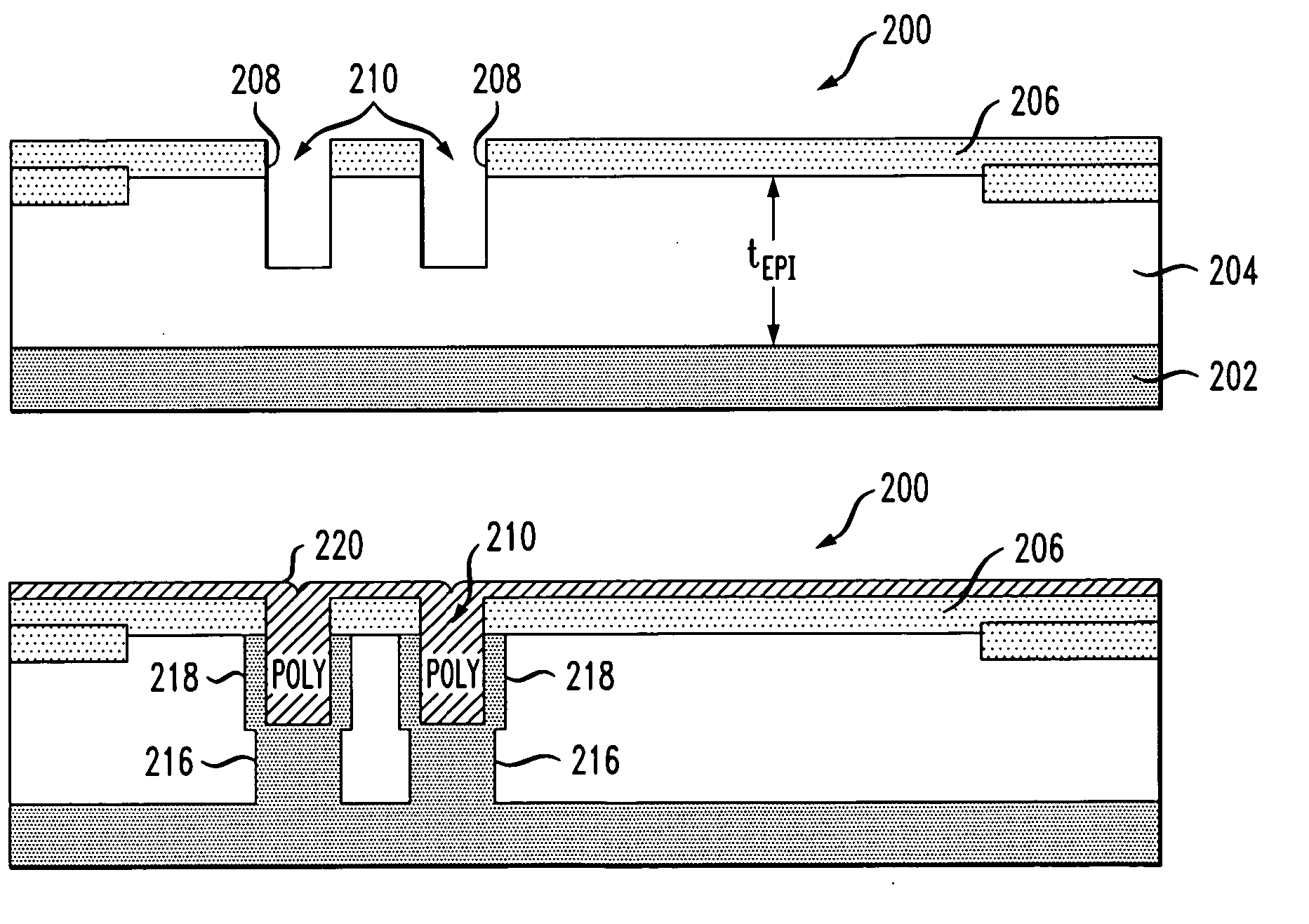
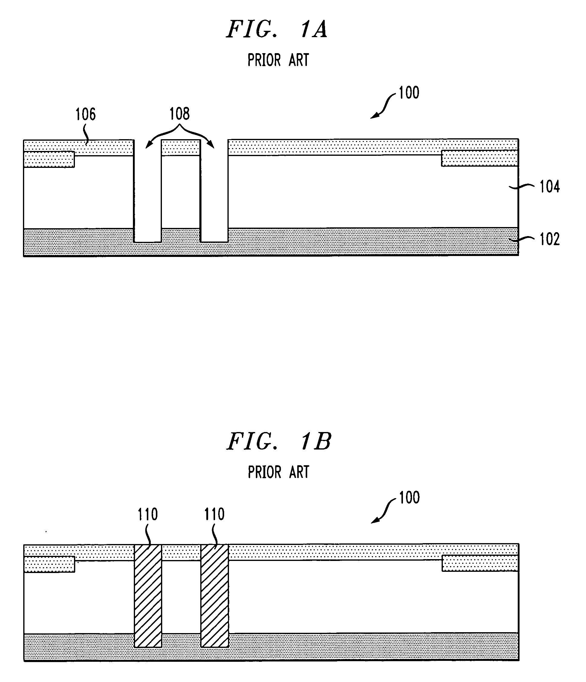
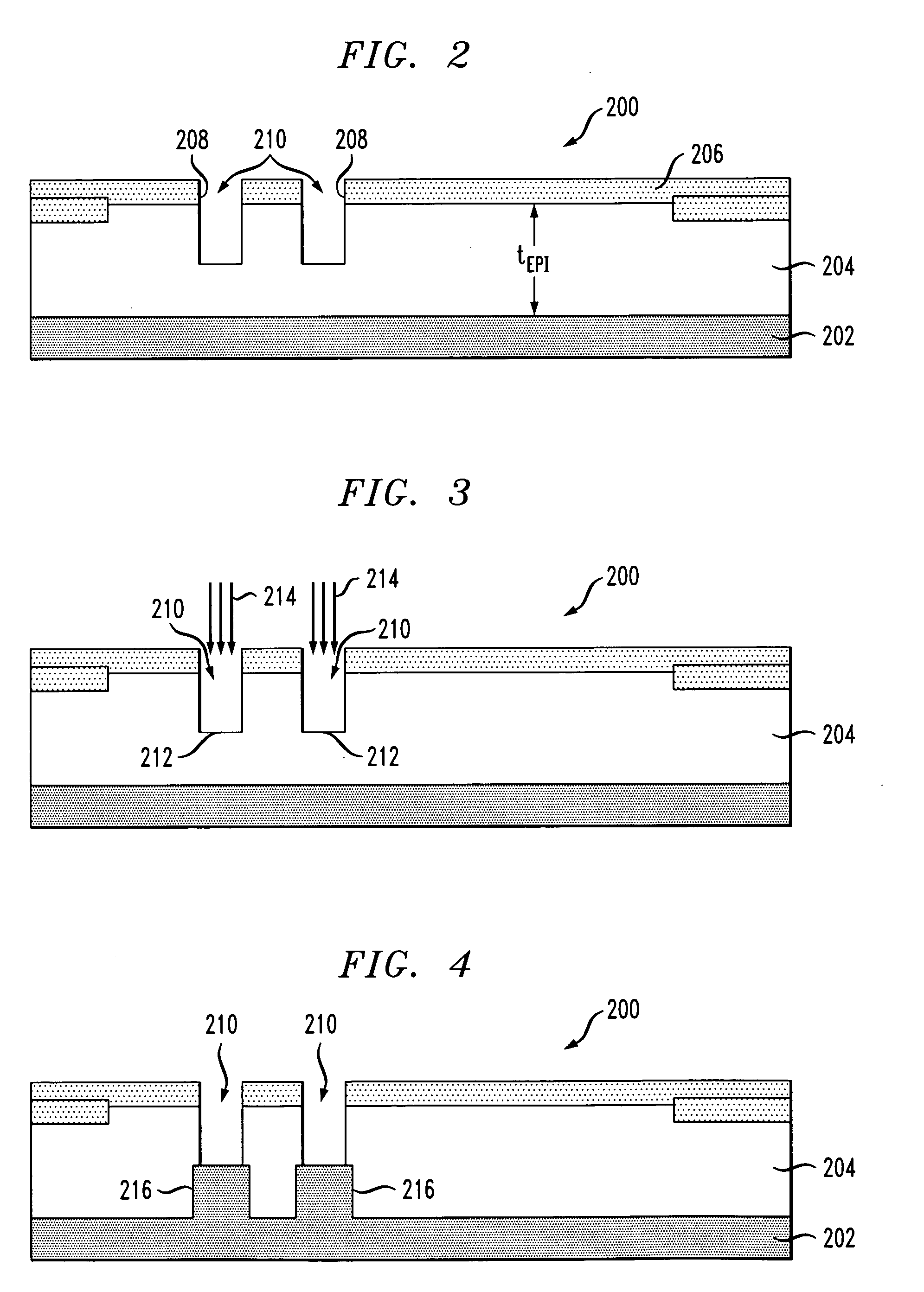
[0016] The present invention will be described herein in the context of an illustrative MOS integrated circuit fabrication technology suitable for forming discrete RF LDMOS transistors, as well as other devices and / or circuits. It should be appreciated, however, that the present invention is not limited to the fabrication of this or any particular device or circuit. Rather, the invention is more generally applicable to techniques for forming a semiconductor structure capable of providing a low-resistance electrical connection between an upper surface of an epitaxial layer and a substrate associated with a semiconductor wafer. Moreover, although implementations of the present invention are described herein with specific reference to an LDMOS device and a complementary metal-oxide-semiconductor (CMOS) fabrication process, it is to be appreciated that the techniques of the present invention are similarly applicable to other fabrication processes (e.g., bipolar) and / or the formation of ...


PUM


Abstract

A technique for forming a semiconductor structure in a semiconductor wafer includes the steps of forming an epitaxial layer on a least a portion of a semiconductor substrate of a first conductivity type and forming at least one trench in an upper surface of the semiconductor wafer and partially into the epitaxial layer. The method further includes the step of forming at least one diffusion region between a bottom wall of the trench and the substrate, the diffusion region providing an electrical path between the bottom wall of the trench and the substrate. One or more sidewalls of the trench are doped with a first impurity of a known concentration level so as to form an electrical path between an upper surface of the epitaxial layer and the at least one diffusion region. The trench is then filled with a filler material.

Description

FIELD OF THE INVENTION [0001] The present invention relates generally to semiconductor devices, and more particularly relates to techniques for forming a substrate contact for use in a semiconductor device. BACKGROUND OF THE INVENTION [0002] Power metal-oxide-semiconductors (MOS) devices, including lateral diffused MOS (LDMOS) devices, are employed in a variety of applications, such as, for example, power amplifiers in wireless communications systems. Radio frequency (RF) LDMOS devices are generally fabricated on a semiconductor wafer comprising a substrate that is typically formed of single crystal silicon which has been heavily doped with an impurity, such as, for example, boron, so as to form a low-resistivity substrate (e.g., about 1018 to about 1019 atoms per cubic centimeter). A lightly-doped epitaxial layer (e.g., about 1014 to about 1015 atoms per cubic centimeter), typically about ten microns thick, is generally formed on the substrate. [0003] One problem in fabricating an ...

Claims


Application Information

Patent Timeline
Patent Type & Authority Applications(United States)
IPC IPC(8): H01L21/20H01L21/336H01L29/417
CPCH01L29/4175H01L29/66659
Inventor BAIOCCHI, FRANK A.JONES, BAILEY R.SHIBIB, MUHAMMED AYMANXU, SHUMING
Owner BELL SEMICON LLC
Why Eureka
Try Eureka