Plasma processing apparatus and method

a plasma processing apparatus and plasma technology, applied in the direction of plasma technique, vacuum evaporation coating, coating, etc., can solve the problems of unstable electric discharge, difficult to start electric discharge (plasma ignition) or sustain electric discharge, and electrons from the electric field given, etc., to achieve stable electric discharge, simple and low cost structure, and easy to start rf discharge

Active Publication Date: 2005-10-13
TOKYO ELECTRON LTD
View PDF8 Cites 19 Cited by
  • Summary
  • Abstract
  • Description
  • Claims
  • Application Information

AI Technical Summary

Benefits of technology

[0010] An object of the present invention is to provide a plasma processing apparatus and method, which can easily start RF discharge and stably sustain the electric discharge with a simple and low cost structure.

Problems solved by technology

In such a plasma processing apparatus utilizing RF discharge, as the gas pressure is set low, the density of gas molecules becomes low, thereby making it difficult to start electric discharge (plasma ignition) or sustain the electric discharge.
Particularly, where the plasma processing apparatus is of a parallel-plate type, this characteristic is prominent, and, even if the inter-electrode gap is set smaller, or the RF voltage applied across the electrodes is set lager, the energy given to electrons from the electric field, i.e., energy for ionizing gas molecules or atoms, is insufficient, thereby likely making electric discharge unstable.
However, since the ignition plasma method uses conditions different from the main process conditions for a certain period of time, there are some disadvantages in that the process is affected and the throughput is reduced.
Similarly, as regards the method employing microwaves or UV rays, there are also some problems in that the process may be affected, and the apparatus becomes complex, which increases the apparatus cost.

Method used


Image

  • Plasma processing apparatus and method
  • Plasma processing apparatus and method
  • Plasma processing apparatus and method

Examples


Embodiment Construction

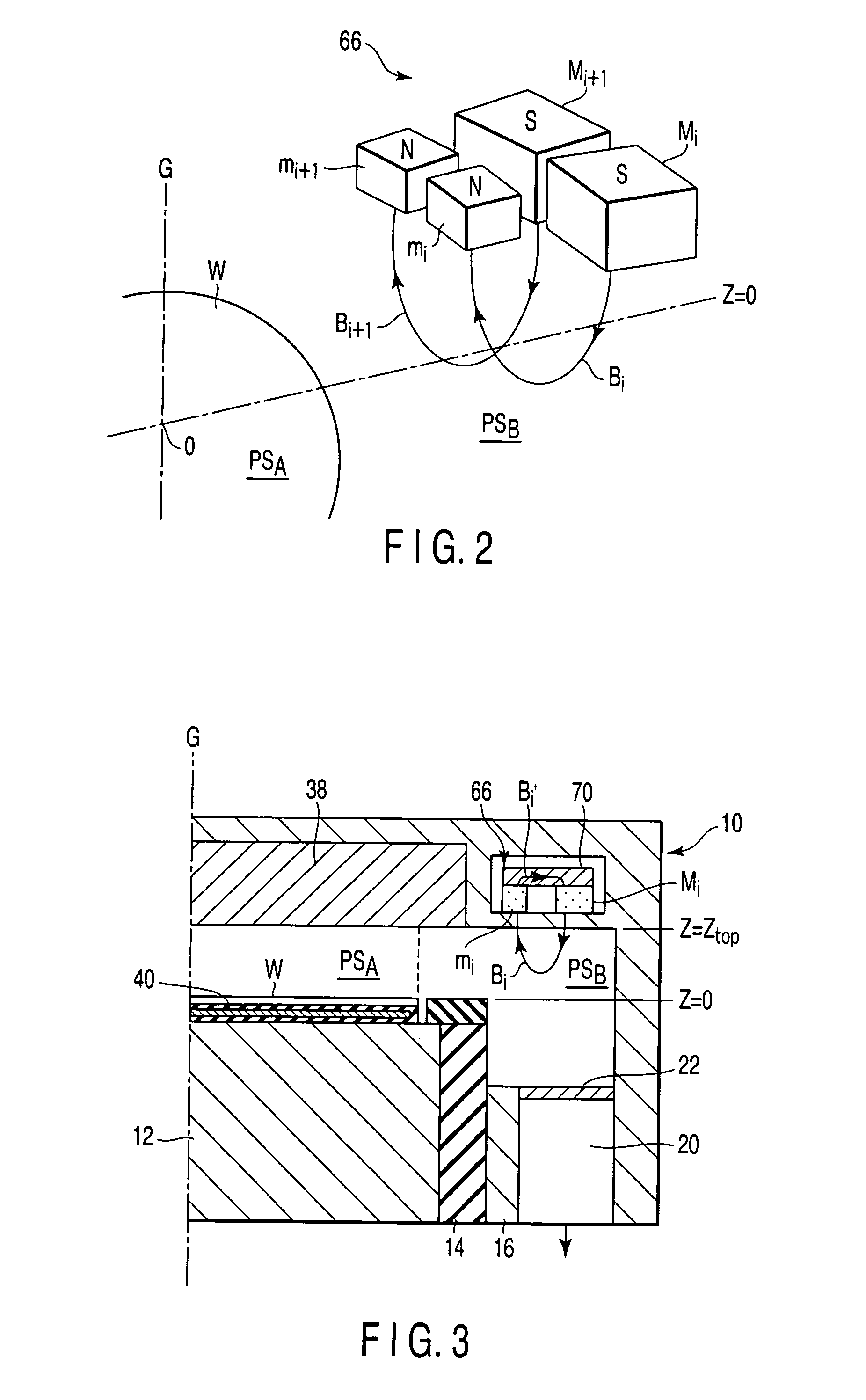
[0047] Embodiments of the present invention will now be described with reference to the accompanying drawings. In the following description, the constituent elements having substantially the same function and arrangement are denoted by the same reference numerals, and a repetitive description will be made only when necessary.

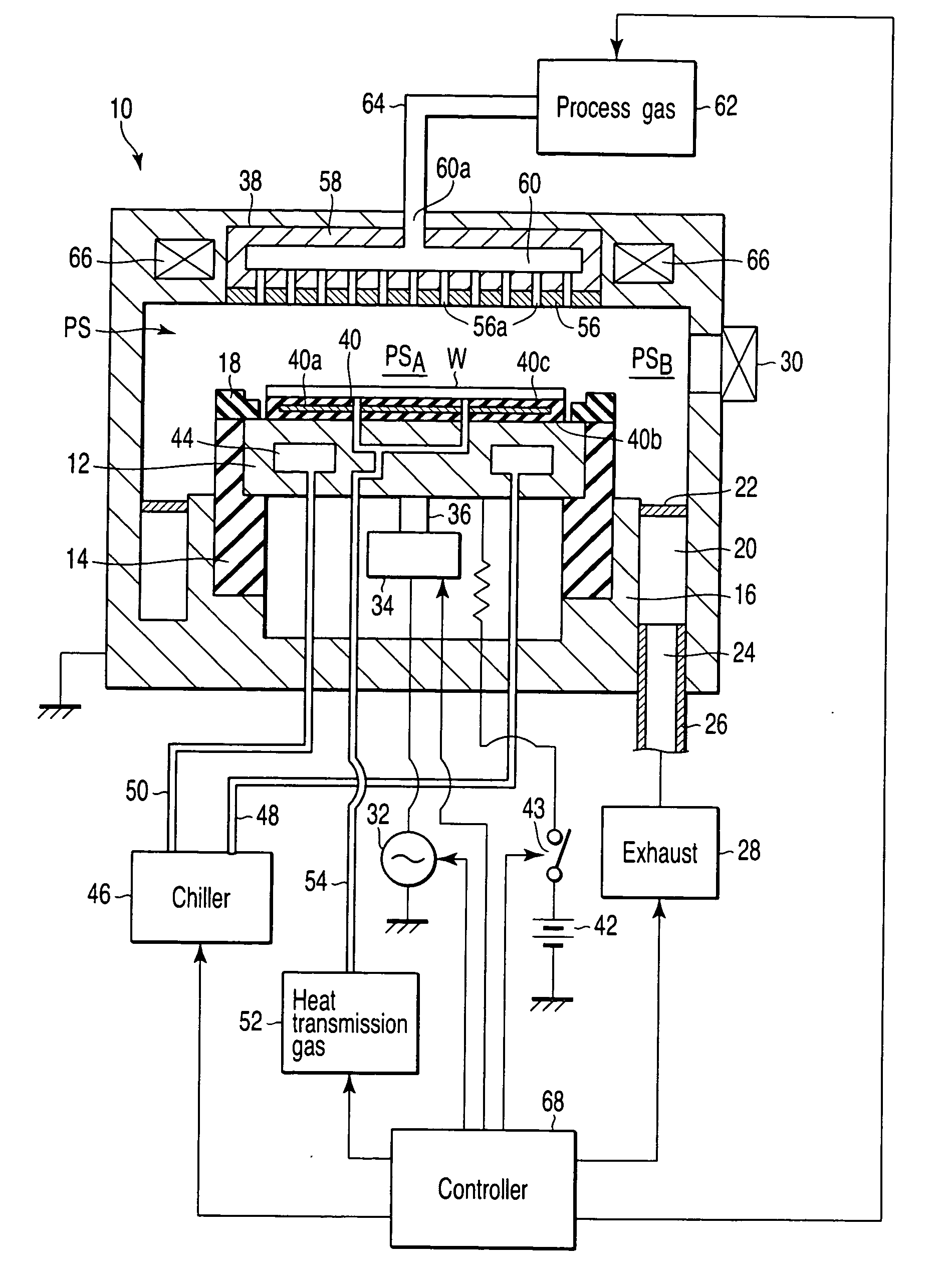
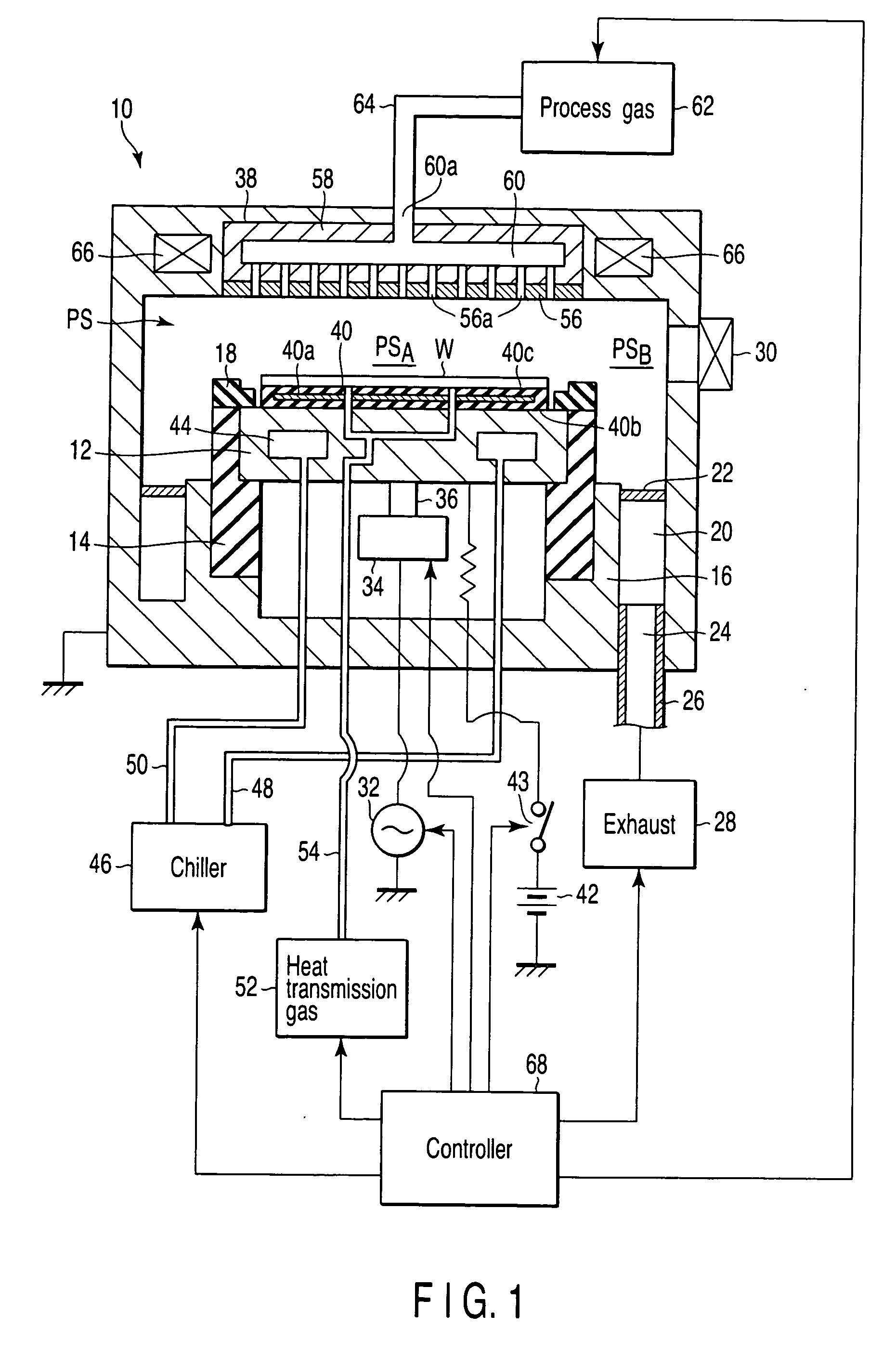
[0048]FIG. 1 is a sectional view showing a plasma processing apparatus for a semiconductor process according to an embodiment of the present invention. This plasma processing apparatus is structured as a plasma etching apparatus of a parallel-plate type. The plasma etching apparatus includes a cylindrical process chamber (process container) 10, which is made of a metal, such as aluminum or stainless steel, and is protectively grounded.

[0049] The process chamber 10 is provided with a circular lower electrode or susceptor (worktable) 12 disposed therein, on which a target substrate or semiconductor wafer W is placed. The susceptor 12 is made of, e.g., aluminum, ...


PUM

PropertyMeasurementUnit
frequencyaaaaaaaaaa
magnetic fieldaaaaaaaaaa
diameteraaaaaaaaaa

Abstract

A plasma processing apparatus includes a worktable in a process chamber to horizontally place a target substrate thereon. A plasma generation space is defined above and around the worktable within the process chamber. The plasma generation space includes a peripheral plasma region and a main plasma region respectively located outside and inside an outer edge of the target substrate placed on the worktable. The apparatus further includes a magnetic field forming mechanism configured to form a magnetic field within the peripheral plasma region. The magnetic field includes magnetic force lines extending through the peripheral plasma region between a start position and an end position, at least one of which is located radially inside a sidewall of the process chamber.

Description

CROSS-REFERENCE TO RELATED APPLICATIONS [0001] This application is based upon and claims the benefit of priority from prior Japanese Patent Application No. 2004-114240, filed Apr. 8, 2004, the entire contents of which are incorporated herein by reference. BACKGROUND OF THE INVENTION [0002] 1. Field of the Invention [0003] The present invention relates to an apparatus and method for performing a plasma process on a target substrate, and particularly to a semiconductor processing apparatus and method of the single substrate type which utilize radio frequency (RF) discharge to generate plasma. The term “semiconductor process” used herein includes various kinds of processes which are performed to manufacture a semiconductor device or a structure having wiring layers, electrodes, and the like to be connected to a semiconductor device, on a target substrate, such as a semiconductor wafer or a glass substrate used for an LCD (Liquid Crystal Display) or FPD (Flat Panel Display), by forming ...

Claims


Application Information

Patent Timeline
Patent Type & Authority Applications(United States)
IPC IPC(8): C23C14/32H05H1/16C23C16/509H01J37/32H01L21/00H01L21/205H01L21/3065H05H1/46
CPCH01J37/32623H01J37/3266H01L21/3065H01L21/205
Inventor IWASAKI, MASAHIDEUKEI, TOMOAKI
Owner TOKYO ELECTRON LTD
Why Eureka
Try Eureka