Methods of eliminating pattern collapse on photoresist patterns

Inactive Publication Date: 2005-10-13
MICRON TECH INC
View PDF8 Cites 69 Cited by
  • Summary
  • Abstract
  • Description
  • Claims
  • Application Information

AI Technical Summary

Benefits of technology

[0005] The present invention provides a stabilizing solution for treating photoresist patterns to prevent profile abnormalities, toppling and resist footing. The stabilizing solution comprises a non-volatile component, such as non-volatile particles or polymers, which is applied after the photoresist material has been developed. By treating the photoresist with the s

Problems solved by technology

Surface tension pulls down the walls of the photoresist (also known as toppling) during the rinsing and drying steps of the development process, therefore destroying the pattern that was originally formed.
When the walls

Method used


Image

  • Methods of eliminating pattern collapse on photoresist patterns
  • Methods of eliminating pattern collapse on photoresist patterns
  • Methods of eliminating pattern collapse on photoresist patterns

Examples


example 1

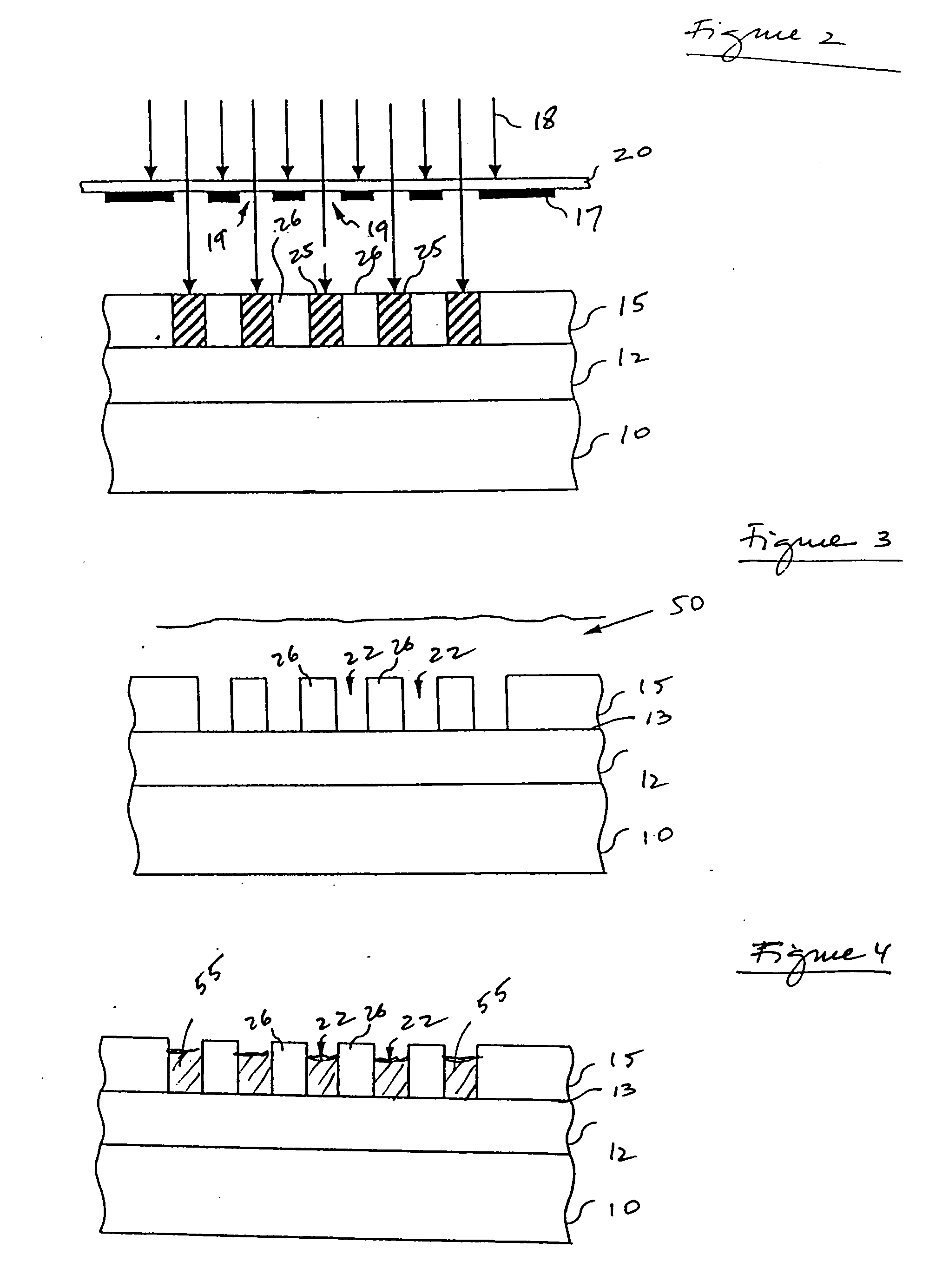
[0047] A bare silicon wafer was processed with 2800A AR360 resist on 450A Dongjin Barc and exposed with a reticle at standard exposure / focus. The wafer received a standard post-exposure bake. The wafer was subsequently developed and rinsed in a dump rinse tank, and then pulled out from the tank and placed horizontally. A Klebesol slurry using silica particles was applied to the wafer before the drying process could induce collapse (toppling) of the patterns 26a (FIG. 6). The time from the pulling out of the tank of the wafer to applying the Klebesol slurry was preferably under 10 seconds, to avoid collapse of the patterns.

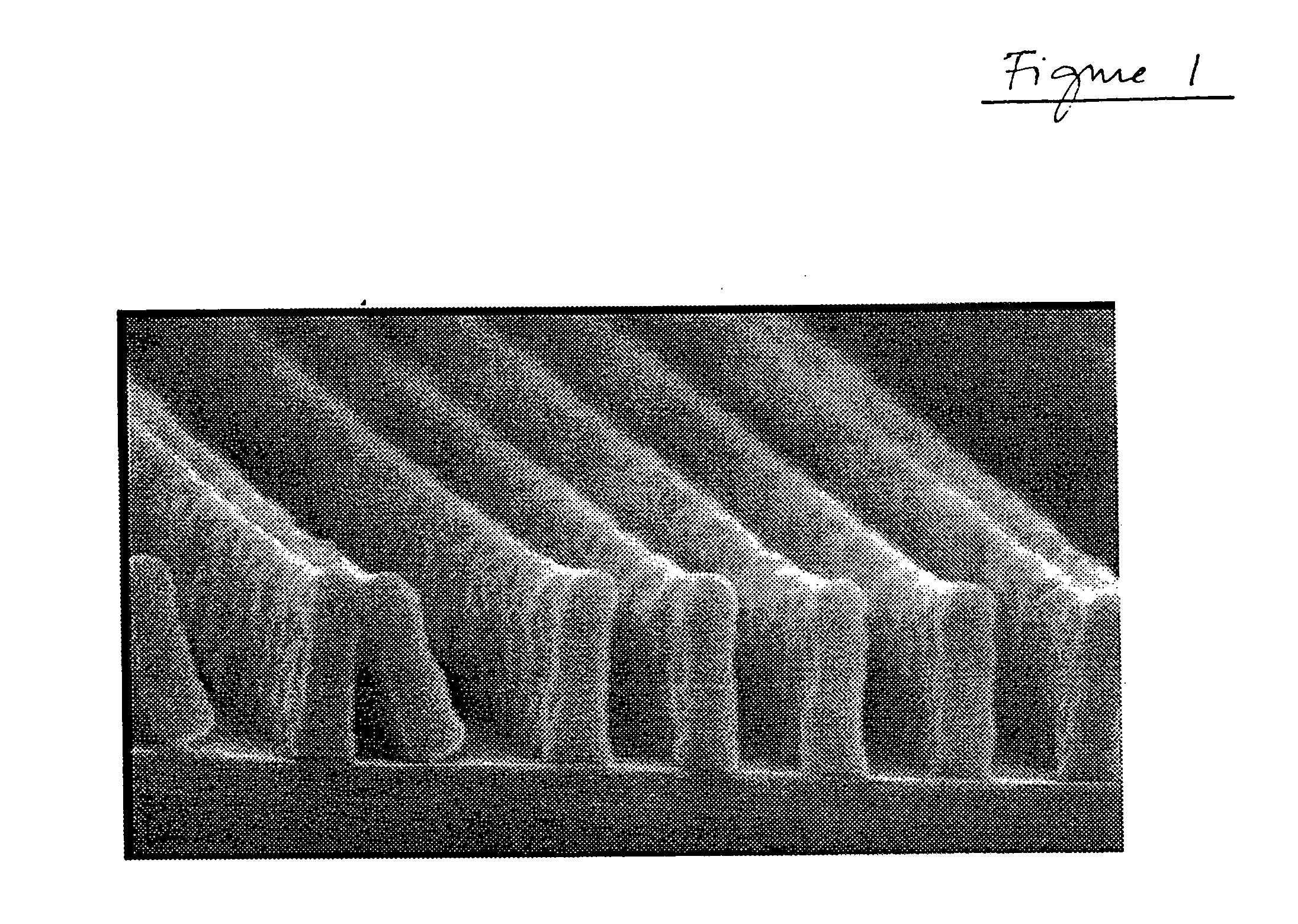
[0048]FIG. 6 is a photograph illustrating silica particles 55a of the Klebesol slurry physically supporting resist lines 26a without collapse, fabricated as detailed in Example 1. As shown in FIG. 6, the resist lines 26a have a vertical and substantially defect-free profile, with virtually no pattern collapse and no resist footing or profile abnormalities. The sil...

example 2

[0057] A bare silicon wafer was processed with 2000A AR360 resist from JSR on 450A Dongjin Barc. After the resist formation, the wafer was baked at a temperature of about 130° C. for about 90 seconds and then exposed on an ASML scanner PAS1100. The wafer was baked again, at a temperature of about 130° C. for about 90 seconds. The wafer was subsequently developed with ARCH 4262 developer for about 30 seconds. While spinning the developer on the wafer, a TOK FSC050 polymer solution was added by spin coating to displace the developer. The wafer was rinsed in a dump rinse tank, and then pulled out from the tank and baked at a temperature of about 170° C. for about 60 seconds. After the baking, a de-ionized (DI) water rinse was applied.

[0058]FIG. 10 is a photograph illustrating resist pattern lines 126a without profile abnormalities and without toppling, fabricated as detailed in Example 2 above. As shown in FIG. 10, the resist lines 126a have a vertical and substantially defect-free pr...


PUM


Abstract

A stabilizing solution for treating photoresist patterns and methods of preventing profile abnormalities, toppling and resist footing are disclosed. The stabilizing solution comprises a non-volatile component, such as non-volatile particles or polymers, which is applied after the photoresist material has been developed. By treating the photoresist with the solution containing a non-volatile component after developing but before drying, the non-volatile component fills the space between adjacent resist patterns and remains on the substrate during drying. The non-volatile component provides structural and mechanical support for the resist to prevent deformation or collapse by liquid surface tension forces.

Description

FIELD OF THE INVENTION [0001] The invention relates to the fabrication of electronic components such as integrated circuit semiconductors and, in particular, to methods for avoiding resist pattern collapse in the photolithography steps of integrated circuit fabrication. BACKGROUND OF THE INVENTION [0002] Photolithographic patterning is a well-established technology in the manufacturing processes of various kinds of semiconductor devices and liquid crystal display panels. According to photolithographic patterning, a photosensitive resist composition is first coated onto a surface of a substrate to form a photoresist layer. The photoresist layer is then exposed to radiation, such as ultraviolet light or electron beam, so that some portions of the photoresist are impacted by radiation while other portions of the photoresist are not impacted by the radiation. Subsequently, the photoresist is subjected to a developer solution, which selectively removes either the impacted or non-impacted...

Claims


Application Information

Patent Timeline
IPC IPC(8): G03F7/40H01L23/58
CPCG03F7/40H01L21/0335
Inventor DALEY, JONHISHIRO, YOSHIKI
Owner MICRON TECH INC
Why Eureka
Try Eureka