Intersubband mid-infrared electroluminescent semiconductor devices

a semiconductor and mid-infrared technology, applied in semiconductor lasers, laser details, electrical equipment, etc., can solve the problems of low power conversion efficiency (0.5%), only at wavelengths around 9 m, and the inability to operate cw, and achieve the effect of suppressing carrier leakag

Active Publication Date: 2005-10-13
WISCONSIN ALUMNI RES FOUND
View PDF20 Cites 14 Cited by
  • Summary
  • Abstract
  • Description
  • Claims
  • Application Information

AI Technical Summary

Benefits of technology

[0007] In the present invention, intersubband semiconductor light emitting devices are provided which virtually suppress carrier leakage to the continuum by utilizing very deep active quantum wells sandwiched between very high barrier layers. For GaAs-based devices, for example, In0.3Ga0.7As active layer quantum wells can be sandwiched between Al0.8Ga0.2As barrier layers to provide the very deep quantum wells. In addition, because GaAs / AlGaAs superlattices do not need to be used on both sides of the active region, resonant tunneling cannot occur between X valleys at high transition energies, and thus room temperature emission in the mid-IR range becomes possible for GaAs-based devices and other semiconductor laser devices.

Problems solved by technology

More recently continuous wave (CW) operation has been achieved at 300 K, but with very low power conversion efficiency (<0.5%) and only at wavelengths around 9 μm.
Despite this rapid improvement in the performance capabilities of GaInAs / InP-based quantum cascade lasers, it is unlikely that they will ever be able to operate CW at 300 K with high power conversion efficiency (>15%) at wavelengths of interest in the mid-infrared (3 to 5 μm) and far-infrared (8 to 12 μm) wavelength ranges due primarily to the fact that their radiative efficiency is inherently poor.
Fabrication of devices with complicated structures of this type is both difficult and relatively expensive.
Furthermore, for such devices the necessary impurity doping in the superlattice injectors causes a significant increase in the room-temperature threshold current density due to excited carriers from the superlattice reflector / transmitter regions that fill the lower levels of prior active regions, thus reducing the population inversion.

Method used


Image

  • Intersubband mid-infrared electroluminescent semiconductor devices
  • Intersubband mid-infrared electroluminescent semiconductor devices
  • Intersubband mid-infrared electroluminescent semiconductor devices

Examples


Embodiment Construction

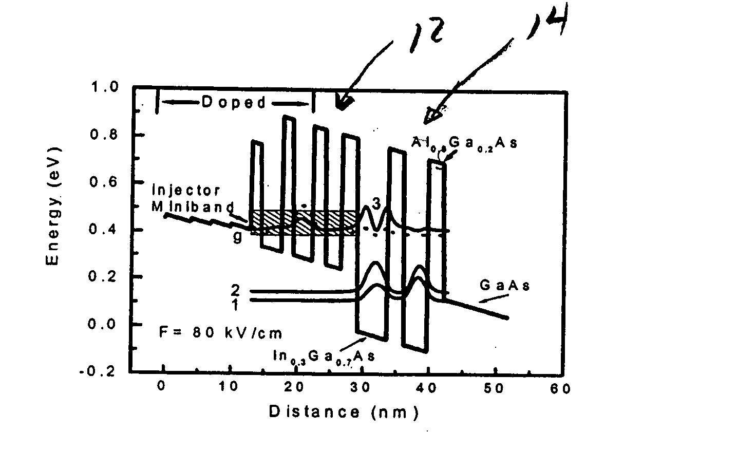
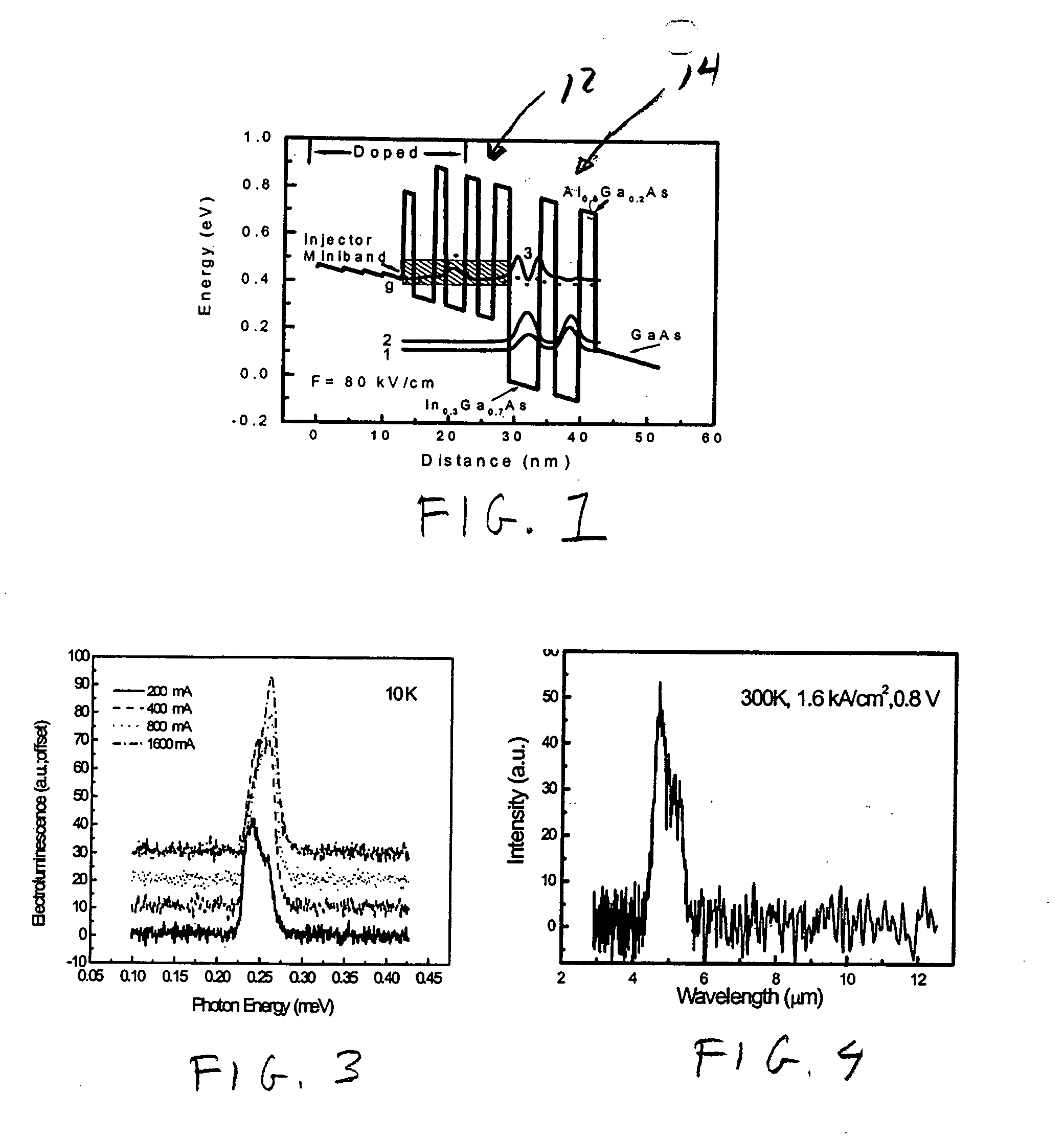
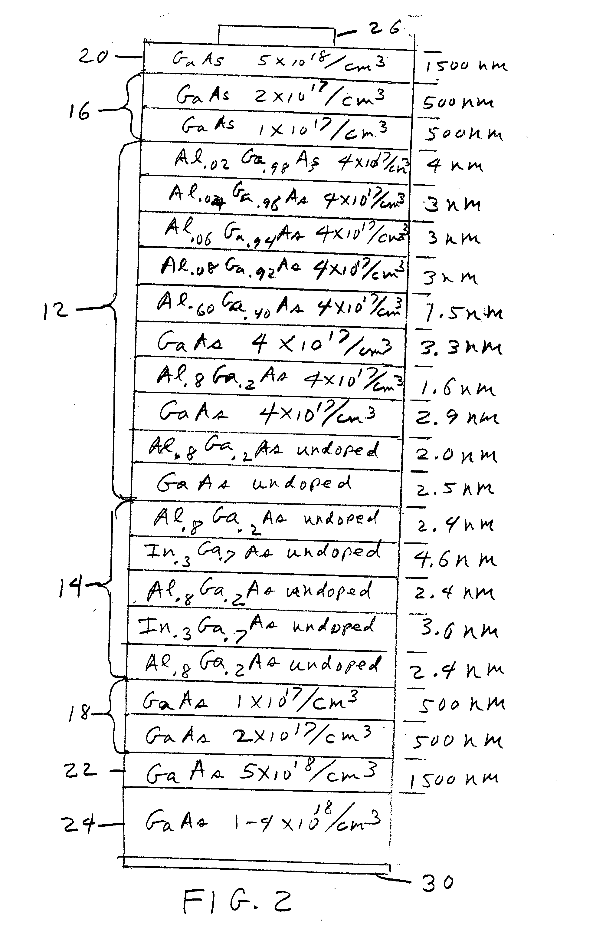
[0020] For purposes of exemplifying the invention, a conduction band energy diagram of an injector region 12 and a double quantum well (DQW) active region 14 for a device in accordance with the invention is shown in FIG. 1. The injector 12 and the DQW active region 14 are inserted in the middle of a plasmon-enhanced n-GaAs waveguide. See, S. Barbieri, et al., 2001, supra, and C. Sirtori, 2002, supra. FIG. 1 shows the moduli squared of the relevant wave functions (solid curves for the n=3, n=2 and n=1 states and a dotted curve for the g state). The injector region is n-type doped (4×1017 cm−3) over the indicated range, and corresponds to a donor sheet density of 3.7×1011 cm−2 in the superlattice section. A simplified cross-section of the layers in the transverse direction is shown in FIG. 2, with exemplary compositions, doping levels, and thicknesses of the various layers indicated thereon. As illustrated in FIG. 2, the injector 12 and the active region 14 are formed between a GaAs u...


PUM


Abstract

A semiconductor laser and light emitting device is defined. The device comprises an electron injector and an active region adjacent to the electron injector. The active region includes at least one deep quantum well with barrier layers adjacent to either side of the quantum well or wells such that electrons injected from the electron injector into a high energy level of the quantum well relax to a lower energy level with the emission of a photon and are transmitted out to a region beyond the last barrier layer of the active region. The electron injector includes quantum well layers. The bottom of each deep quantum well or wells in the active region is lower in energy than the bottoms of the quantum well layers in the electron injector. The device may further comprise at least two stages wherein each stage contains an electron injector and an active region. The stages are separated by semiconductor layers that allow the transfer of electrons from the active region of one stage to the electron injector of the next stage.

Description

CROSS-REFERENCE TO RELATED APPLICATION [0001] This application claims the benefit of provisional patent application No. 60 / 533,635, filed Dec. 31, 2003, the disclosure of which is incorporated herein by reference.STATEMENT OF GOVERNMENT RIGHTS [0002] This invention was made with United States government support awarded by the following agency: DOD ARPA N66001-03-1-8900. The United States government has certain rights in this invention.FIELD OF THE INVENTION [0003] This invention pertains generally to the field of semiconductor lasers and light emitting devices and particularly to intersubband semiconductor light emitters. BACKGROUND OF THE INVENTION [0004] Semiconductor lasers are formed of multiple layers of semiconductor materials. The conventional semiconductor diode laser typically includes an n-type layer, a p-type layer and an undoped layered active structure between them such that when the diode is forward biased electrons and holes recombine within the active structure with ...

Claims


Application Information

Patent Timeline
Patent Type & Authority Applications(United States)
IPC IPC(8): H01S5/00H01S5/30H01S5/34H01S5/343
CPCB82Y20/00H01S5/305H01S5/34313H01S5/3402H01S5/3419H01S5/3054
Inventor BOTEZ, DANMIRABEDINI, ALI R.XU, DAPENG P.MAWST, LUKE J.
Owner WISCONSIN ALUMNI RES FOUND
Why Eureka
Try Eureka