
Semiconductor device and manufacturing method thereof

a technology of semiconductor devices and semiconductors, applied in semiconductor devices, electrical devices, transistors, etc., can solve the problems of difficult to improve both the characteristics of current amplification factor and early voltage, disadvantageous lowering of early voltage and the withstand voltage of emitters/collectors, and remarkable foregoing disadvantages, etc., to achieve the effect of short tim

Inactive Publication Date: 2005-10-20
PANASONIC CORP
View PDF0 Cites 0 Cited by
  • Summary
  • Abstract
  • Description
  • Claims
  • Application Information

AI Technical Summary

Benefits of technology

[0026] According to the foregoing constitution, the characteristic of the MOS transistor and the characteristic of the bipolar transistor are independent from each other because the impurity concentration of the source / drain diffusion layer in the MOS transistor and the emitter impurity concentration are different to each other. Therefore, the high-performance semiconductor device of the BiCMOS structure capable of obtaining a high current amplification factor without undermining the characteristic of the MOS transistor and reducing the Early voltage and the emitter / collector withstand voltage in the bipolar transistor can be provided.
[0029] According to the foregoing constitution, the characteristic of the bipolar transistor and the characteristic of the MOS transistor are independent from each other. Therefore, the high-performance semiconductor device of the BiCMOS structure capable of obtaining a high current amplification factor without undermining the characteristic of the MOS transistor and reducing the Early voltage and the emitter / collector withstanding voltage in the bipolar transistor can be provided. As a further advantage, the impurities can be additionally introduced into the polycrystal silicon emitter layer at the same time as the formation of the source / drain diffusion layer of the MOS transistor. As a result, the high-performance bipolar transistor of a self-aligning type can be formed without increasing a manufacturing cost.
[0036] According to the foregoing manufacturing method, the polycrystal silicon emitter layer is used as the diffusion source so as to form the emitter diffusion layer, and the impurities are additionally introduced into the polycrystal silicon emitter layer and activated at a temperature lower than the temperature at which the emitter diffusion layer is formed after the formation of the emitter diffusion layer. As a result, the concentration of the impurities additionally introduced into the polycrystal silicon emitter layer can be adjusted. Further, the emitter impurity concentration can be increased without changing the depth of the emitter diffusion layer, and the current amplification factor can be easily controlled separately from the Early voltage and the emitter / collector withstand voltage, which realizes a high current amplification factor.
[0047] In the foregoing method of manufacturing the semiconductor device, the step of additionally introducing the impurities into the polycrystal silicon emitter layer is preferably carried out at the same time as the step of introducing the impurities into the well layer. The high-performance bipolar transistor of the self-aligning type can be formed without increasing the manufacturing cost as a result of additionally introducing the impurities into the source / drain diffusion layer of the MOS transistor at the same time as the formation of the polycrystal silicon emitter.
[0049] In the foregoing method of manufacturing the semiconductor device, the step of forming the emitter diffusion layer is preferably carried out at a high temperature and in a short period of time by means of a lamp annealing treatment.

Problems solved by technology

It is possible to increase the current amplification factor by raising the impurity concentration of the polycrystal silicon emitter layer, in which case, however, the Early voltage and the emitter / collector withstand voltage are disadvantageously lowered as a result of the deepened diffusion.
As described, the characteristic of the current amplification factor and the characteristic of the Early voltage are in a trade-off relationship, which makes it difficult to improve both of the characteristics of the current amplification factor and the Early voltage.
In particular, in the case of a bipolar transistor of PNP type, the foregoing disadvantage is even more remarkable because the emitter diffusion layer is formed through the solid phase diffusion using boron having a large diffusion coefficient.

Method used


Image

  • Semiconductor device and manufacturing method thereof
  • Semiconductor device and manufacturing method thereof
  • Semiconductor device and manufacturing method thereof

Examples


embodiment 1

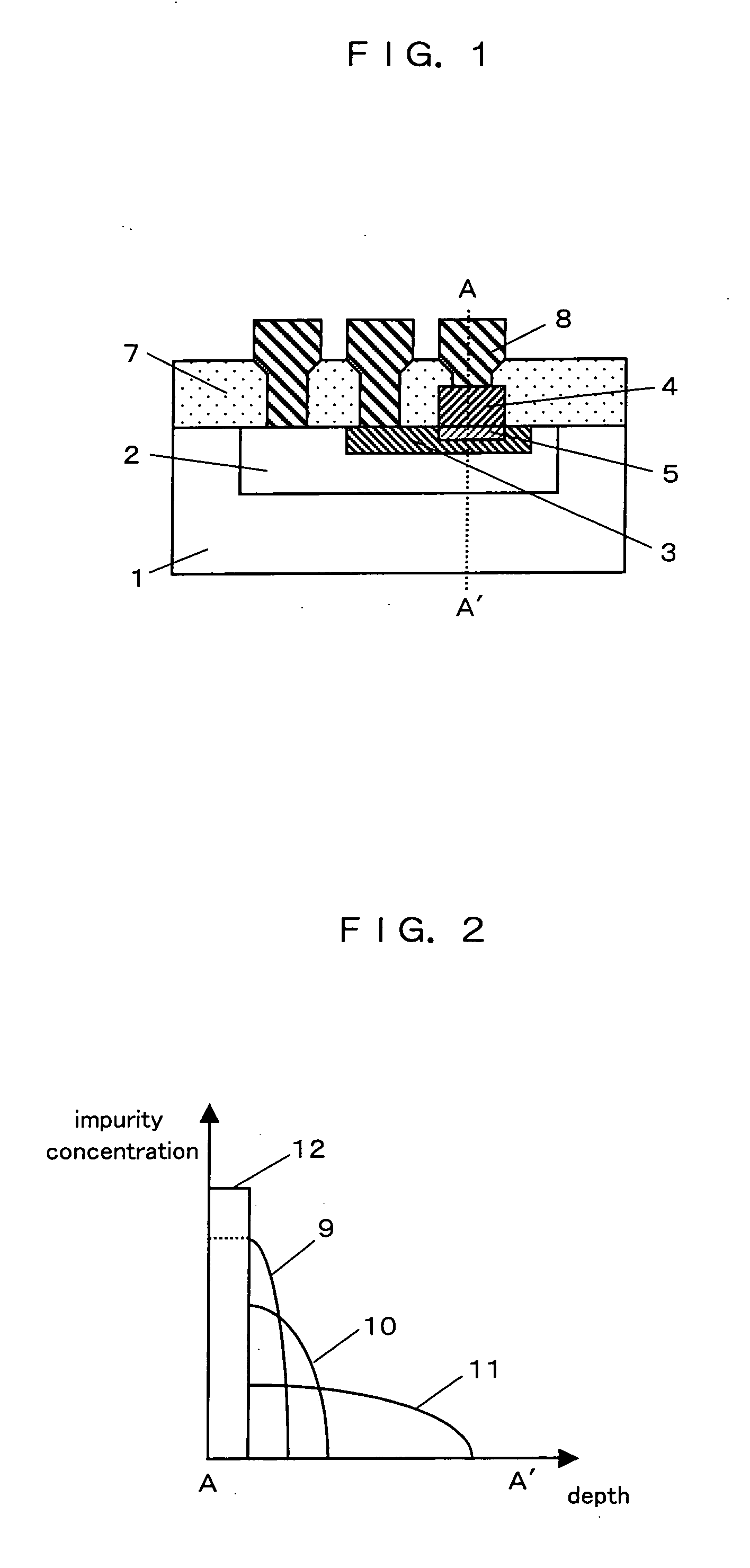
[0061]FIG. 1 is a sectional view of a semiconductor device of a bipolar structure having a bipolar transistor of PNP type according to an embodiment 1 of the present invention. FIG. 2 is a distribution chart of an impurity concentration of A-A′ part in FIG. 1.

[0062] As shown in FIG. 1, a P-type collector diffusion layer 2 is formed in a semiconductor substrate 1, an N-type base diffusion layer 3 is formed in the P-type collector diffusion layer 2, and a P-type emitter diffusion layer 5 is formed in the base diffusion layer 3 using a polycrystal silicon emitter layer 4 including boron as a diffusion source. Further, an insulation film 7 is deposited on the respective diffusion layers, and the respective diffusion layers are connected to wirings 8 via contact holes.

[0063] Referring to reference numerals in FIG. 2, 9 denotes a distribution of a P-type impurity concentration of the emitter diffusion layer, 10 denotes a distribution of an N-type impurity concentration of the base diffu...

embodiment 2

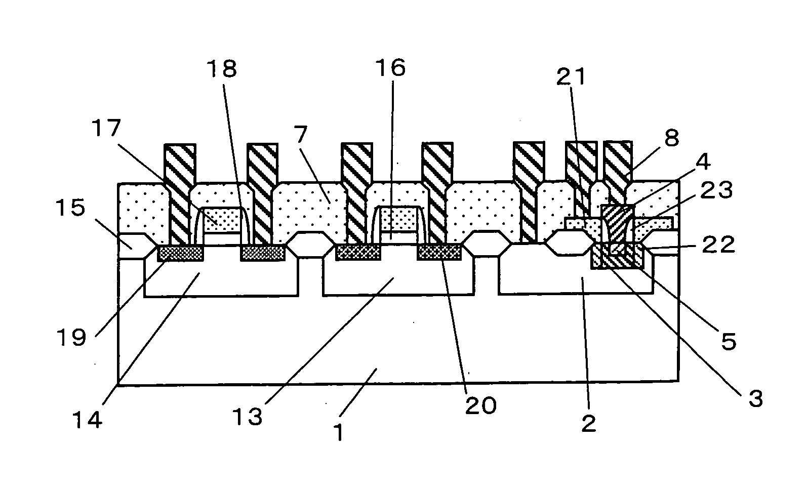
[0072]FIG. 4 is a sectional view of a semiconductor device of a BiCMOS structure having a PNP-type bipolar transistor and a CMOS transistor according to an embodiment 2 of the present invention.

[0073] As shown in FIG. 4, a P-type collector diffusion layer 2 is formed in a semiconductor substrate 1, an N-type base diffusion layer 3 is formed in the P-type collector diffusion layer 2, and a P-type emitter diffusion layer 5 is formed in the base diffusion layer 3 using a polycrystal silicon emitter layer 4 including boron as a diffusion source. Referring to PMOS and NMOS transistors, a polycrystal silicon gate electrode 17 including phosphorous P is formed on an N-type well layer 13 and a P-type well layer 14 via a gate insulation film 16, and a P-type source / drain diffusion layer 20 and an N-type source / drain diffusion layer 19 are respectively formed in the N-type well layer 13 and P-type well layer 14. An insulation film 7 is deposited on the respective diffusion layers, and the re...

embodiment 3

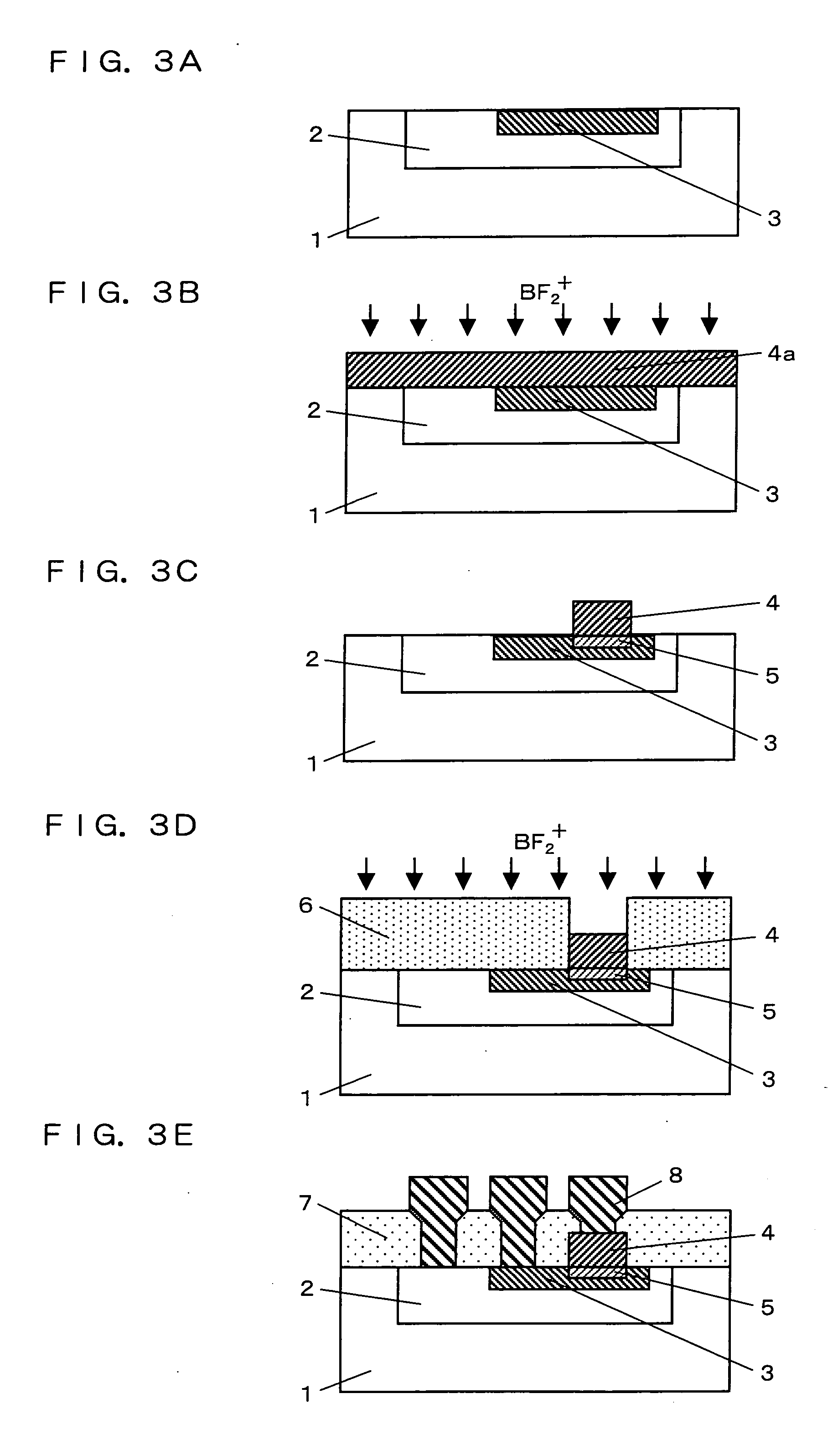
[0084] Respective steps in a method of manufacturing a semiconductor device of a BiCMOS structure having a PNP-type bipolar transistor and a CMOS transistor according to an embodiment 3 of the present invention are shown in sectional views of FIGS. 7A-7D and 8A-8C. The present embodiment is different to the embodiment 2 in that a polycrystal silicon gate electrode of the MOS transistor and a polycrystal silicon external base layer of the bipolar transistor are formed from the same polycrystal silicon.

[0085] First, as shown in FIG. 7A, an N-type well layer 13 and a P-type well layer 14 are respectively formed in a semiconductor substrate 1 having an N-type epitaxial layer on a surface thereof by ion-implanting phosphorous and boron. The P-type collector diffusion layer 2 is formed at the same time as the formation of the P-type well layer 14.

[0086] Next, as shown in FIG. 7B, a field oxide film 15 for determining the element region is formed on the surface of the semiconductor subst...


PUM


Abstract

In a semiconductor device according to the present invention, an emitter diffusion layer is formed with a polycrystal silison emitter layer serving as a diffusion source, and an impurity concentration of the polycrystal silicon emitter layer is higher than an impurity concentration of the emitter diffusion layer, wherein the emitter diffusion layer is of a shallow junction and an emitter impurity concentration is increased.

Description

BACKGROUND OF THE INVENTION [0001] 1. Field of the Invention [0002] The present invention relates to a semiconductor device and a method of manufacturing the semiconductor, more particularly to a semiconductor device provided with a polycrystal silicon emitter layer and a method of manufacturing the semiconductor device. [0003] 2. Description of the Related Art [0004] In recent years, a higher speed has been increasingly advanced in a semiconductor integrated circuit, in response to which it is now demanded that a bipolar transistor be operated in a high-frequency region by downsizing elements, and also, a current amplification factor be increased. In order to do so, it becomes necessary to promote a shallow junction and a high density in a base diffusion layer, and further, to reduce a resistance of an emitter layer. To respond to the demand, a semiconductor device in which an emitter electrode and a base electrode are formed in a self-aligning structure has been proposed and made ...

Claims


Application Information

Patent Timeline
IPC IPC(8): H01L21/331H01L21/8222H01L21/8238H01L21/8248H01L21/8249H01L27/06H01L29/732
CPCH01L21/8249H01L29/732H01L27/0623
Inventor IWADATE, HIDENORIKURIYAMA, HITOSHIYOSHIZAWA, MASAO
Owner PANASONIC CORP
Learn More