Dry etching method and semiconductor device
a technology of semiconductor devices and etching methods, which is applied in the direction of semiconductor devices, solid-state devices, decorative arts, etc., can solve the problems of affecting device characteristics, easy damage to silicon semiconductor layers, and susceptible to plasma etching damage, etc., and achieves the effect of suppressing surface damage and high ra
- Summary
- Abstract
- Description
- Claims
- Application Information
AI Technical Summary
Benefits of technology
Problems solved by technology
Method used
Image

Examples
first embodiment
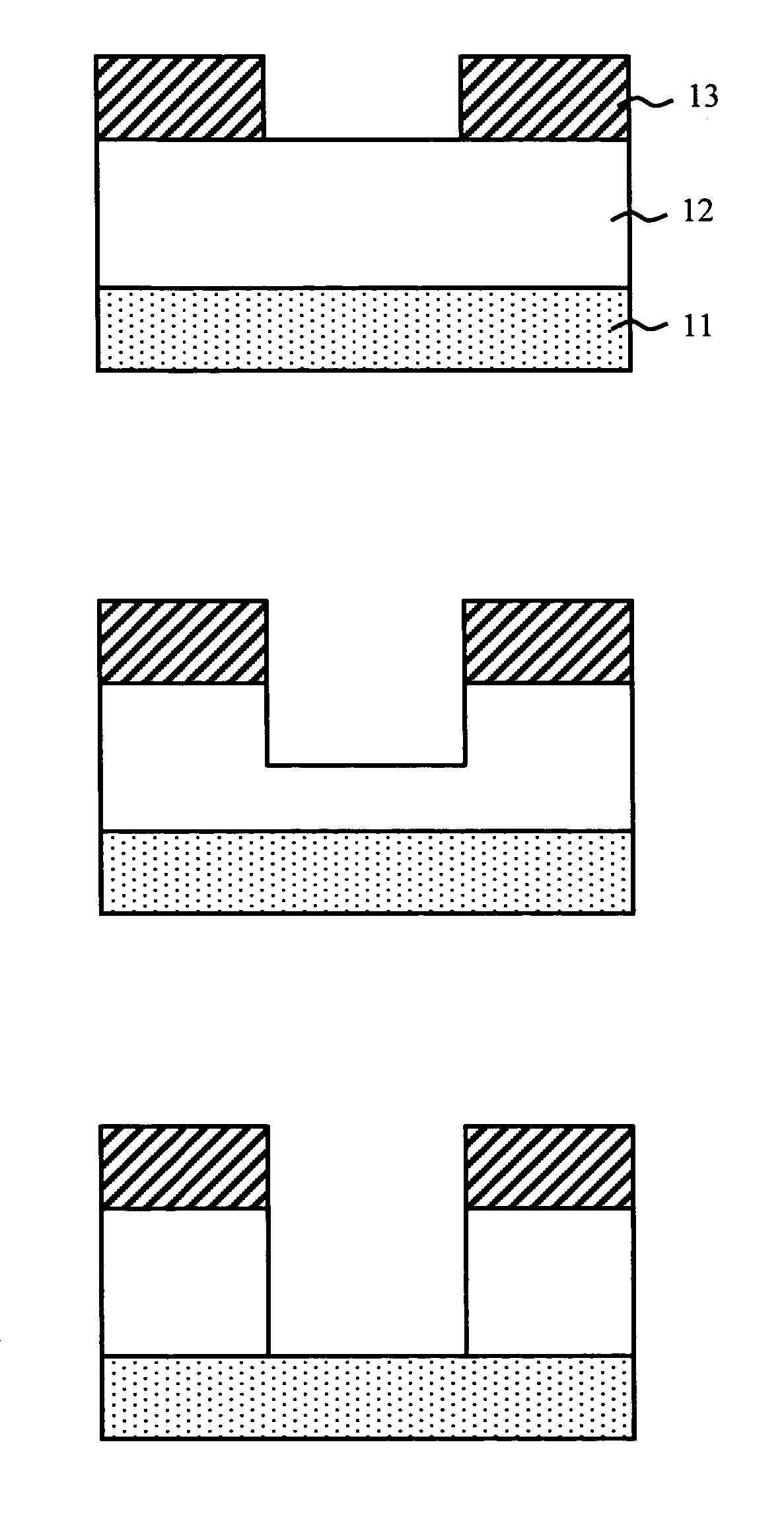
[0039] A description will be given of an example in which the dry etching method of the present invention is applied to a SiNx surface protection film layer provided on a GaN based semiconductor layer in accordance with a first embodiment of the present invention.
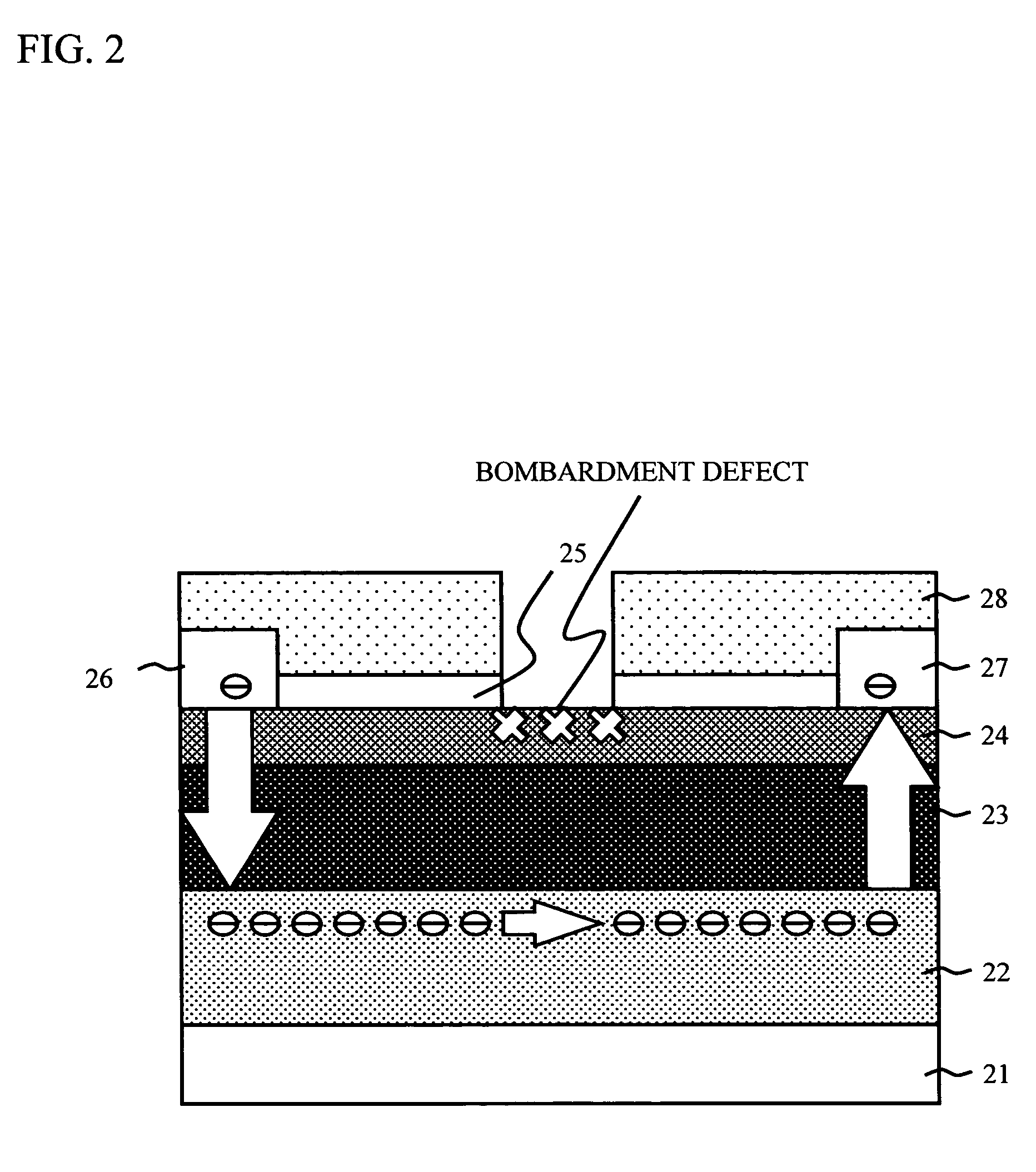
[0040]FIG. 2 is a cross-sectional view of a GaN based HEMT device to be etched by the dry etching method of the present invention and illustrates how a bombardment defect occurs if the conventional dry etching method is employed.
[0041] This device includes a substrate 21 made of any one of SiC, sapphire, and GaN. An electron traveling layer 22 of GaN, an electron supply layer 23 of n-type AlGaN, and a surface protection thin-film layer 24 of n-type GaN are sequentially provided on the substrate 21. In addition, a protection film 25 of SiNx, a source 26, and a drain 27 are provided on the surface protection thin-film layer 24. A window substance 28 coats the protection film 25, the source 26, and the drain 27. The window s...
second embodiment
[0049] A description will be given of an example in which the dry etching method of the present invention is applied to a GaN surface protection film layer provided on an AlGaN layer.
[0050]FIG. 5 is a cross-sectional view of a GaN based HEMT device to be etched by the dry etching method of the present invention and illustrates how the bombardment defect occurs if the conventional dry etching is performed.
[0051] This device includes a substrate 51 of any one of SiC, sapphire, and GaN. An electron traveling layer 52 of GaN, and an electron supply layer 53 of n-type AlGaN are sequentially deposited on the substrate 51. In addition, a surface protection thin-film layer 54 of n-type GaN, a source 55, and a drain 56 are provided on the electron supply layer 53. The surface protection thin-film layer 54, the source 55, and the drain 56 are coated by a window substance 57. The window substance 57 serves as a mask when the gate is formed by dry etching. The window substance 57 has an open ...
third embodiment
[0059] A description will be given of an example in which the dry etching method of the present invention is applied to a SiC substrate, which is arranged on a backside of a GaN based vertical cavity surface emitting laser (VCSEL).
[0060]FIG. 8 is a cross-sectional view of a GaN VCSEL device to be dry etched by the dry etching method of the present invention and illustrates how the bombardment defect occurs if the conventional dry etching is performed.
[0061] A GaN based VCSEL 91 includes a GaN thick-film layer 80 provided on the SiC substrate (not shown), a GaN based buffer layer 81, an n-type GaN layer 82, an InGaN layer 83 having a quantum well structure, an AlGaN layer 84 of a current control layer, a p-type GaN contact layer 85, a p-type ohmic electrode 86a, an n-type ohmic electrode 86b, a SiN protection layer 87, a polyamide film 88, and a wiring material 89.
[0062] The p-type ohmic electrode 86a and the n-type ohmic electrode 86b are biased and carriers are injected from the...
PUM
| Property | Measurement | Unit |
|---|---|---|
| Fraction | aaaaa | aaaaa |
| Fraction | aaaaa | aaaaa |
| Fraction | aaaaa | aaaaa |
Abstract
Description
Claims
Application Information
PatSnap Eureka turns technology decisions into work you can execute. Powered by our Innovation Knowledge Graph, it runs expert workflows across engineering, life sciences, materials and intellectual property. Get your review-ready output in minutes.


