

Film bulk acoustic-wave resonator and method for manufacturing the same
a film and acoustic wave technology, applied in the field of film bulk acoustic wave resonators, can solve the problems of difficult to meet the demand for higher frequency of operation, difficult to merge the circuitry of the rf front-end unit into a single lsi chip, and complicated configuration of the rf front-end uni
- Summary
- Abstract
- Description
- Claims
- Application Information
AI Technical Summary
Benefits of technology
Problems solved by technology
Method used
Image

Examples
first embodiment
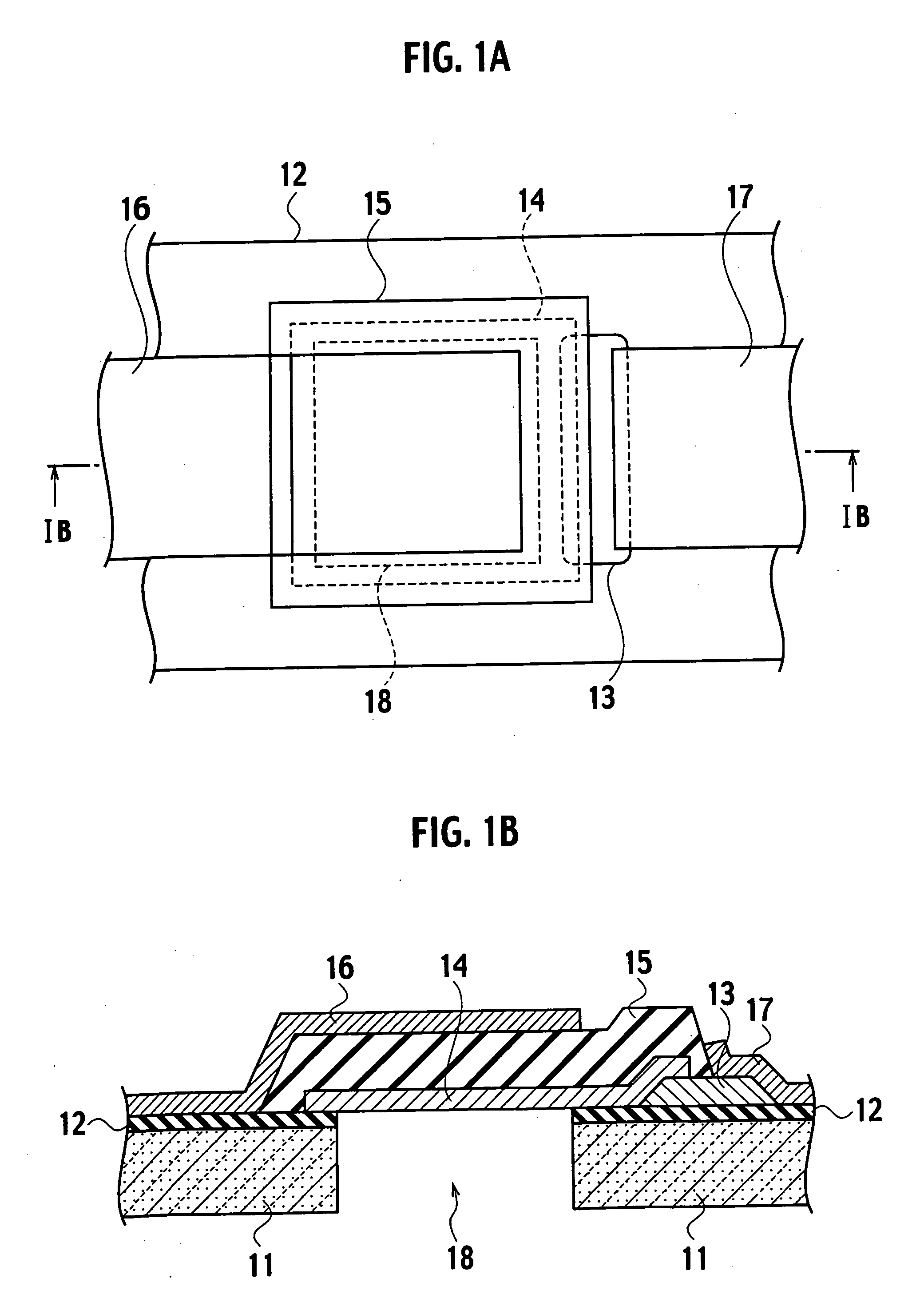
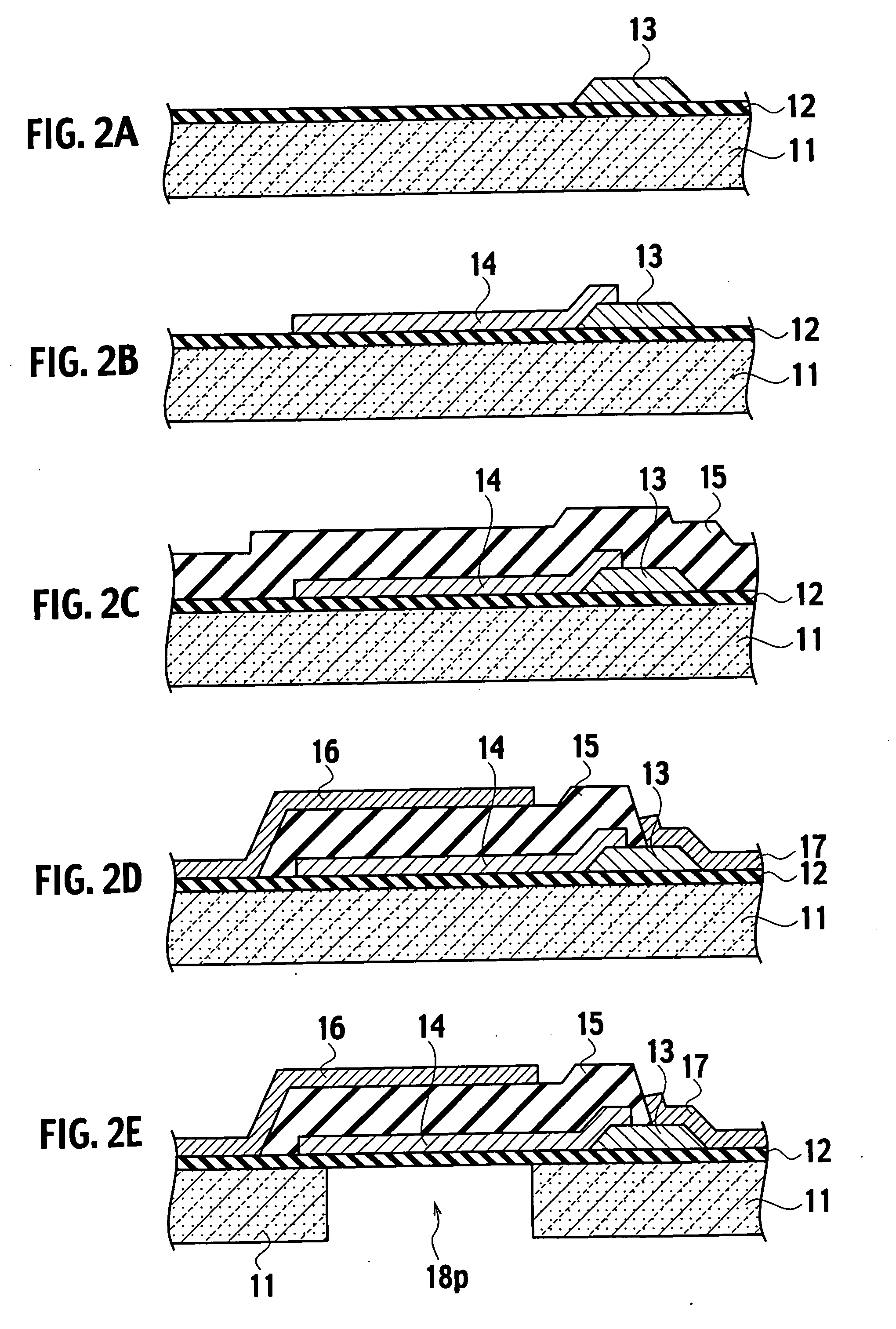
[0087] A film bulk acoustic-wave resonator (FBAR) according to a first embodiment of the present invention encompasses a substrate 11 having a cavity 18, a bottom electrode, part of which is mechanically suspended above the cavity 18 and another part of which is mechanically fixed to the substrate 11, a piezoelectric layer 15 disposed on the bottom electrode, a planar shape of the piezoelectric layer 15 is defined by a contour, which covers an entire surface of the bottom electrode in a plan view shown in FIG. 1A, a top electrode 16 on the piezoelectric layer 15, an intermediate electrode 13 located between the substrate 11 and the piezoelectric layer 15, and at the contour of the piezoelectric layer 15, the intermediate electrode 13 is connected to the bottom electrode in the inside of the contour, and a bottom electrode wiring 17 connected to the intermediate electrode 13 extending from the contour to an outside of the contour in the plan view shown in FIG. 1A The FBAR according t...
second embodiment
[0118] As shown in FIG. 10, a FBAR according to a second embodiment of the present invention includes a substrate 11, an insulating film 12 formed on the substrate 11, a bottom electrode 14, one side of which is fixed to the substrate 11 through the insulating film 12 and the other side of which is mechanically suspended above the insulating film 12 through a trapezoidal cavity 19, a metallic intermediate electrode 13, part of which is disposed on one end of the bottom electrode 14 so as to be electrically connected to the bottom electrode 14, a piezoelectric layer 15 disposed on the bottom electrode 14 and part of the metallic intermediate electrode 13, a top electrode 16 delineated on the piezoelectric layer and a bottom electrode wiring 17 connected to the metallic intermediate electrode 13. FIG. 10 shows a cross-sectional view of the FBAR of the second embodiment. Since a planar pattern of the FBAR is similar to FIG. 1A, the illustration is omitted, the piezoelectric layer 15 co...
third embodiment
[0133] As shown in FIG. 12, a FBAR according to a third embodiment of the present invention includes a substrate 11, an insulating film 12 formed on the substrate 11, an intermediate electrode 23 located such that the intermediate electrode 23 penetrates through the insulating film 12 and is buried into the substrate 11 with a bathtub-shaped (reverse trapezoid) or a U-groove configuration, a bottom electrode 14 disposed on the insulating film 12 and on the intermediate electrode 23, a piezoelectric layer 15 disposed on the bottom electrode 14 and on the intermediate electrode 23, a top electrode 16 delineated on the piezoelectric layer 15 and a bottom electrode wiring 17 connected to the intermediate electrode 23. FIG. 12 shows a cross-sectional view of the FBAR of the third embodiment. Since a planar pattern of the FBAR is similar to FIG. 1A, the illustration is omitted, the piezoelectric layer 15 covers the entire surface of the bottom electrode 14 in the inside of the area define...
PUM
| Property | Measurement | Unit |
|---|---|---|
| Angle | aaaaa | aaaaa |
| Thickness | aaaaa | aaaaa |
| Structure | aaaaa | aaaaa |
Abstract
Description
Claims
Application Information