

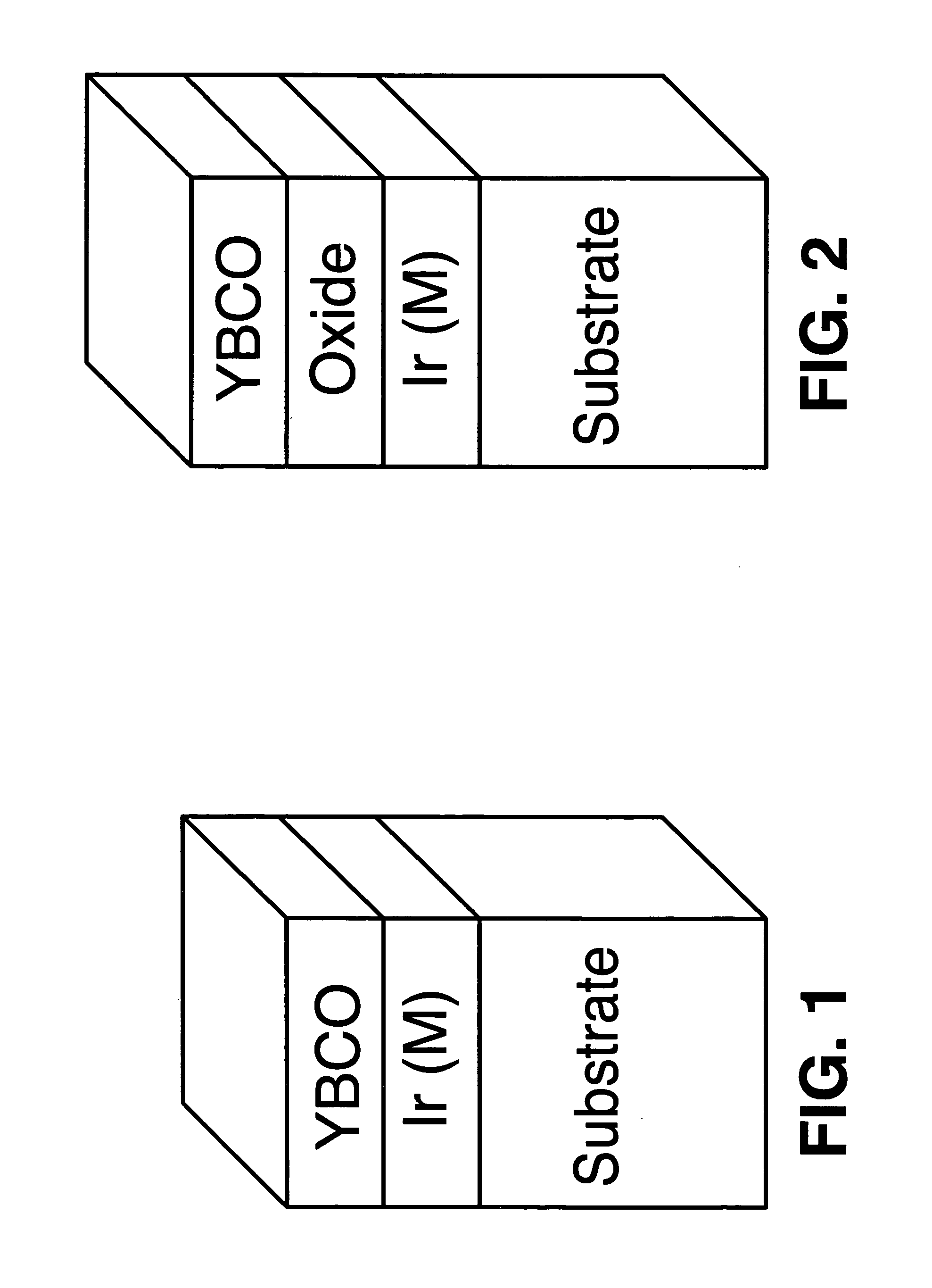
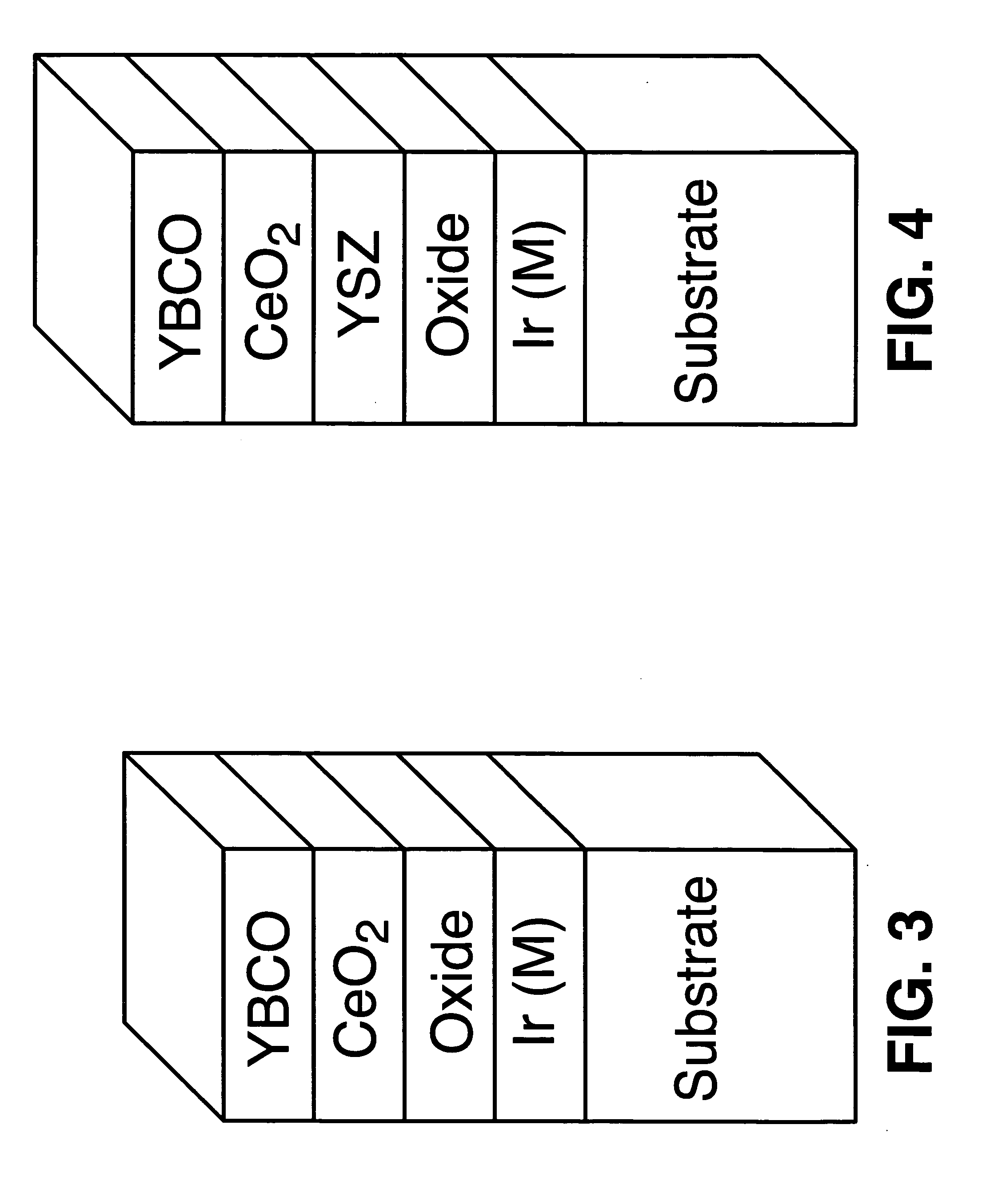
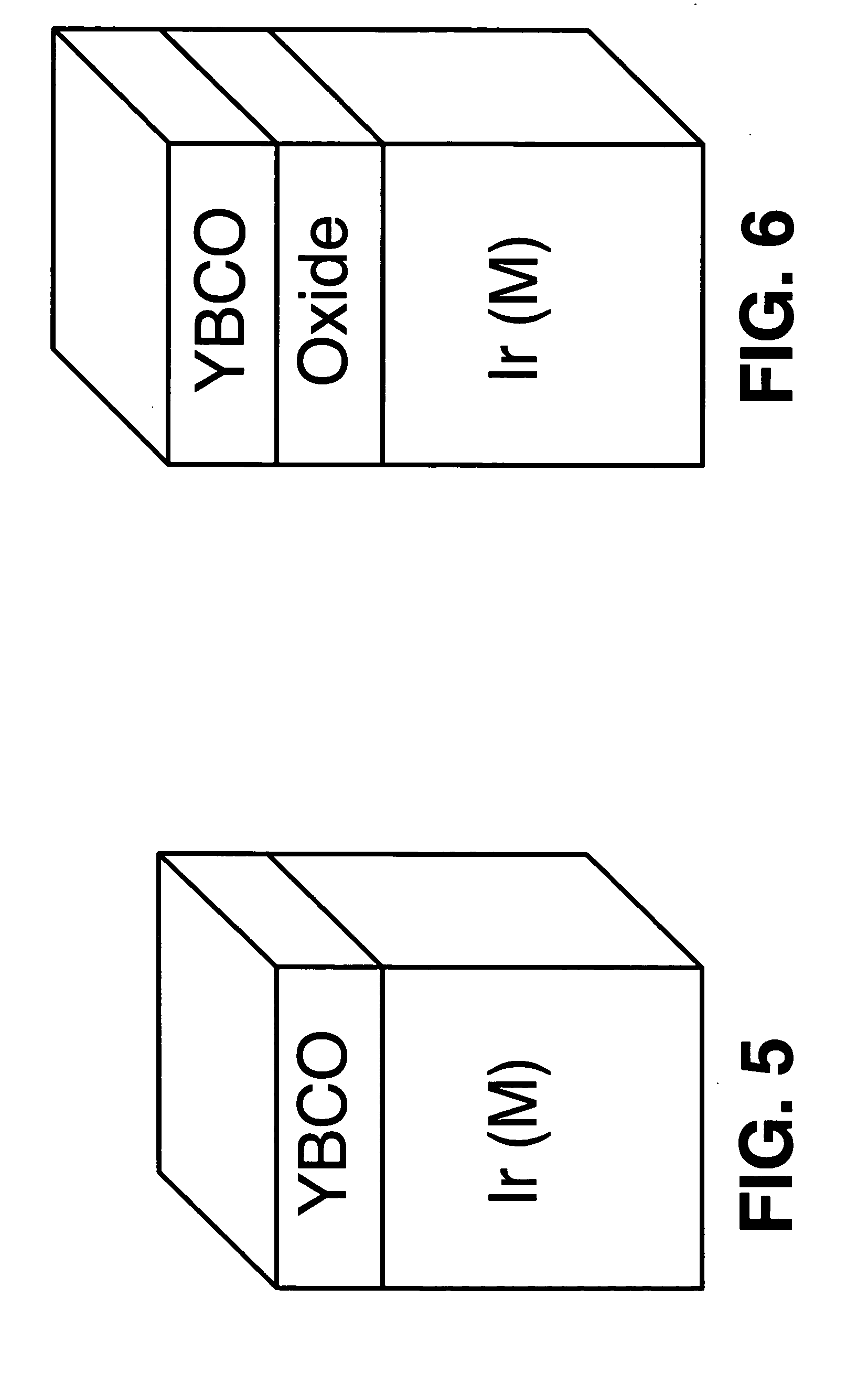
Superconductors on iridium substrates and buffer layers
a technology of superconductors and buffer layers, applied in the direction of superconductors/coils, magnetic bodies, natural mineral layered products, etc., can solve the problems of superconductors being particularly susceptible to problems, superconductors running away, etc., and achieve the effect of reducing ac loss
- Summary
- Abstract
- Description
- Claims
- Application Information
AI Technical Summary
Benefits of technology
Problems solved by technology
Method used
Image

Examples
example i
[0055] Biaxially textured Cu {100} substrates were obtained by mechanical deformation of Cu rods to about a 95% reduction in thickness. This was followed by recrystallization to the desired {100} cube texture by annealing at 800° C. for 1-2 h in a high-vacuum furnace with a base pressure of 2×10⁻⁶ Torr. Similarly, substrates with reduced magnetism, Ni—W (3%) were also produced. The 50 μm thick as-rolled Cu and Ni-alloy substrates were cleaned in isopropanol prior to annealing. After annealing, the Cu substrates were mounted on a heater block using Ag paint and loaded into a vacuum chamber for on-axis sputtering. An Ir metal layer was epitaxially deposited on Cu substrates using dc sputtering of metal target that was 2.0 inches diameter and 0.25 inch thick and a power of ˜100 Watt. Ir layers were deposited at temperatures ranging from 400-700° C. in the presence of Argon and / or Argon-H2 4% gas mixtures. The Ir film thickness was varied in the range of 10-200 nm. The sputtering pressu...
example ii
[0057] La0.7Sr0.3MnO3 (LSMO) buffer layers were deposited on Ir buffered substrates made in accordance with Example I using an rf-magnetron sputtering system with a base pressure of 1×10⁻⁶ Torr, using oxide sputter targets that were 95 mm in diameter and a power of 67 Watt. Unlike sintered and hard-pressed CeO2 and YSZ targets, the LSMO target was made from a single-phase LSMO powder, which was lightly packed into a copper tray. Deposition of LSMO buffer layer was accomplished at substrate temperatures ranging from 550-650° C. in the presence of Argon and / or Argon-H2 (4%) mixture. Oxygen was not added intentionally. In some experiments, water was added into the system to produce stoichiometric LSMO films. The deposition rate was ˜0.71 Å / sec. The LSMO film thickness was varied in the range 200-300 nm to investigate the effect on the microstructure and on the superconducting properties of the subsequent HTS layer. The sputtering pressure was around 3 mTorr. In some experiments, Ir was...
example iii
[0062] Epitaxial Ir buffer layers were deposited ˜100 nm thick, some by sputtering and others by pulsed laser deposition, on biaxially textured Ni—W 3% substrates. Detailed X-ray studies showed that Ir is indeed epitaxial. A typical 0-20 scan for a 100 nm thick Ir buffer layer grown textured Ni—W substrate is shown in FIG. 9. The scan indicates the presence of a c-axis aligned, biaxially textured buffer layer. The buffered substrates were then annealed under YBCO process conditions (i.e., 790° C.; 120 mTorr oxygen pressure, 60 minutes). After the exposure to these conditions, no change was observed in the X-ray pattern. SEM examination revealed no change in microscopic surface features, proving that Ir is stable under YBCO process conditions.
PUM
| Property | Measurement | Unit |
|---|---|---|
| Superconductivity | aaaaa | aaaaa |
Abstract
Description
Claims
Application Information