High speed memory control and I/O processor system

a memory control and high-speed technology, applied in the field of memory control subsystems, can solve the problems of large amount of expensive low density memory technology, large amount of power consumption, and inability to efficiently handle certain memory access patterns, etc., to achieve efficient handling, efficient handling, and efficient handling

Active Publication Date: 2005-10-27
CISCO TECH INC
View PDF8 Cites 439 Cited by
  • Summary
  • Abstract
  • Description
  • Claims
  • Application Information

AI Technical Summary

Benefits of technology

[0013] An input/output processor is designed by analyzing common input/output and memory access patterns and implementing methods tailored to efficiently handle those commonly occurring input/output and memory access patterns. The input/output processor may efficiently handle those common input/output and memory access patterns in a number of different ways.
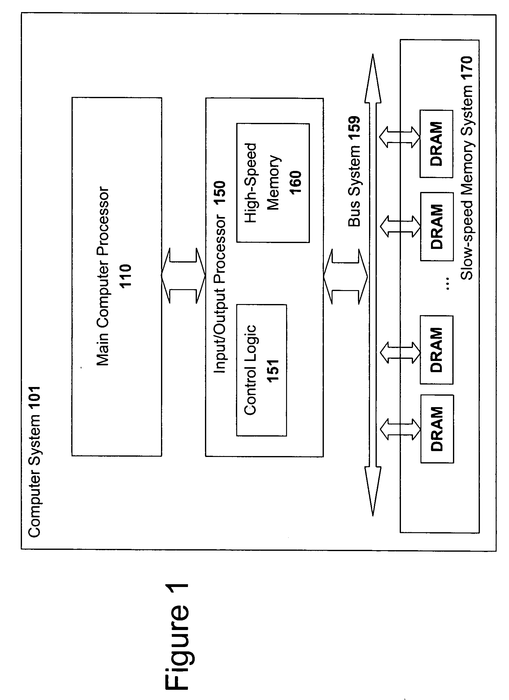
[0014] One technique the input/output processor uses to efficiently handle certain memory access patterns is to off-load some of the processor's work in order to simplify a memory access task. For example, the incrementing of a counter normal requires a processor to read a counter value from memory, increment the counter value, and then write back the incremented counter value back the memory location. The input/output processor instead allows the main processor to issue a single increment counter command with an identifier that specifies a particular counter to increment. The main processor may then resume execution of other commands. The input/output processor will then handle reading the counter value, incrementing the counter, and writing back the counter. Thus, the input/output processor offloads work from the main processor in a manner that reduces the amount of memory accesses performed by the main processor such that its performance is improved.
[0015] Another technique used by the input/output processor is to divide memory storage tasks into high frequency or high-availability components and low frequency or low-availability components. After dividing a memory storage tas...

Problems solved by technology

However, a high-speed computer processor without a matching high-speed memory system that supplies instructions and data just as fast as the processor executes the instructions will eventually become starved of the needed instructions and data.
However, conventional high-speed cache memory systems typically require large amounts expensive low density memory technologies that consume larger amounts of power than standard dynamic random access memory (DRAM).
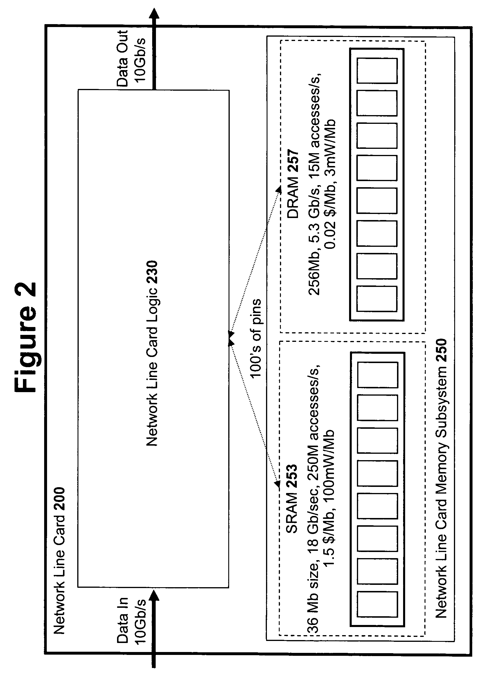
Static random access memory (SRAM) integrated circuits typically cost significantly more than commodity DRAM, consume much more power than DRAM, and are much less dense (less bits per integrated circuit die area) than DRAM.
The most significant drawback of conventional cache memory systems in ...

Method used


Image

  • High speed memory control and I/O processor system
  • High speed memory control and I/O processor system
  • High speed memory control and I/O processor system

Examples


first embodiment

[0285] In the first embodiment, the hybrid memory system stores the first N bytes of each packet in high-speed memory 360. (If there are less than N bytes in the packet then the hybrid memory stores the entire packet in the high-speed memory and pads the remaining bytes with nulls.) After storing the first N bytes, the hybrid memory system then stores the remainder of the packet in blocks of N bytes in the slow-speed memory system 370. For example, with an N value of 150 bytes, the following table lists how various different sized data packets would be divided between the two different memory systems:

Amount stored inAmount stored inPacket Sizehigh-speed memoryslow-speed memory0 to 150 bytes0 to 150 bytes0 bytes151 to 300 bytes150 bytes150 bytes (padded)More than 300 bytes150 bytesMultiples of 150 byteswith last block padded

[0286] When the network processor 310 requests a packet from this first hybrid memory embodiment, the hybrid memory system issues a memory request to both the hig...

second embodiment

[0289] In the second embodiment, the hybrid memory system first identifies the byte location closest to the beginning of the packet wherein the remaining bytes of the packet form even multiples of the N bytes each (if the packet is more than N bytes). The hybrid memory system then stores the beginning of the packet up to identified location in high-speed memory 360. (If the packet is less than N bytes then the entire packet is stored in high-speed memory.) The remainder of the packet (if the packet was more than N bytes) is made up of an even multiple of N bytes. The hybrid memory system stores those remaining packet bytes as blocks of N bytes in the slow-speed memory system 370. For example, with an N value of 150 bytes, the following table lists how various different sized data packets would be divided between the two different memory systems:

Amount stored inAmount stored inPacket Sizehigh-speed memoryslow-speed memory0 to 150 bytes0 to 150 bytes0 bytes151 to 300 bytes0 to 150 byt...


PUM


Abstract

An input/output processor for speeding the input/output and memory access operations for a processor is presented. The key idea of an input/output processor is to functionally divide input/output and memory access operations tasks into a compute intensive part that is handled by the processor and an I/O or memory intensive part that is then handled by the input/output processor. An input/output processor is designed by analyzing common input/output and memory access patterns and implementing methods tailored to efficiently handle those commonly occurring patterns. One technique that an input/output processor may use is to divide memory tasks into high frequency or high-availability components and low frequency or low-availability components. After dividing a memory task in such a manner, the input/output processor then uses high-speed memory (such as SRAM) to store the high frequency and high-availability components and a slower-speed memory (such as commodity DRAM) to store the low frequency and low-availability components. Another technique used by the input/output processor is to allocate memory in such a manner that all memory bank conflicts are eliminated. By eliminating any possible memory bank conflicts, the maximum random access performance of DRAM memory technology can be achieved.

Description

RELATED APPLICATIONS [0001] The present patent application claims the benefit of the previous U.S. Provisional Patent Applications entitled “High Speed Memory Control and I / O Processor System” filed on Dec. 18, 2003 having Ser. No. 60 / 531,043 and entitled “High Speed Packet Buffering System” filed on Feb. 14, 2004 having Ser. No. 60 / 544,883.FIELD OF THE INVENTION [0002] The present invention relates to the field of memory control subsystems. In particular the present invention discloses high-speed memory control system and Input / Output (I / O) processor that can greatly increase the performance of a memory subsystem. BACKGROUND OF THE INVENTION [0003] Digital computer systems generally consist of a short-term memory system, a long-term memory system, a processor, and a set of input / output (I / O) devices for interacting with the outside world. The short-term memory system is generally a volatile memory such as a random access memory that provides for fast access to needed data while the...

Claims


Application Information

Patent Timeline
IPC IPC(8): G06F12/00G06F12/02G06F12/06G06F13/16
CPCG06F12/0223G06F2212/205G06F13/1668G06F12/0607
Inventor IYER, SUNDARMCKEOWN, NICK
Owner CISCO TECH INC
Why Eureka
Try Eureka