Method for manufacturing a panel of a thin film transistor liquid crystal display device

Active Publication Date: 2005-11-03
AU OPTRONICS CORP
View PDF1 Cites 22 Cited by
  • Summary
  • Abstract
  • Description
  • Claims
  • Application Information

AI Technical Summary

Benefits of technology

[0008] The object of the present invention is to provide a method for manufacturing a panel of a thin film transistor liquid cry

Problems solved by technology

When applied to a LCD TV, PM LCD, even a STN LCD, has disadvantages on low response speed and high limitation of colors.
But the TFT LCD is still not

Method used


Image

  • Method for manufacturing a panel of a thin film transistor liquid crystal display device
  • Method for manufacturing a panel of a thin film transistor liquid crystal display device
  • Method for manufacturing a panel of a thin film transistor liquid crystal display device

Examples


Embodiment Construction

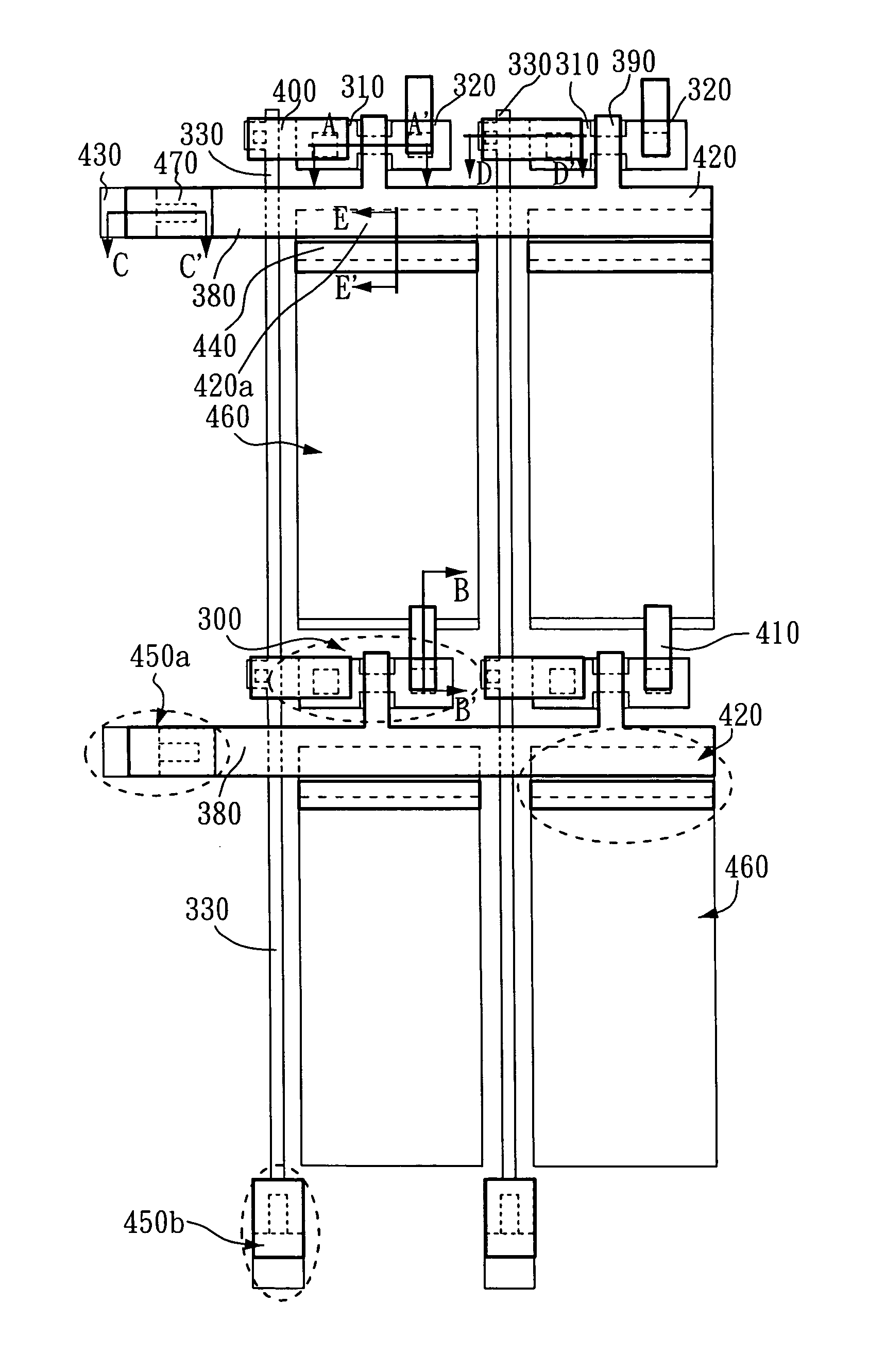
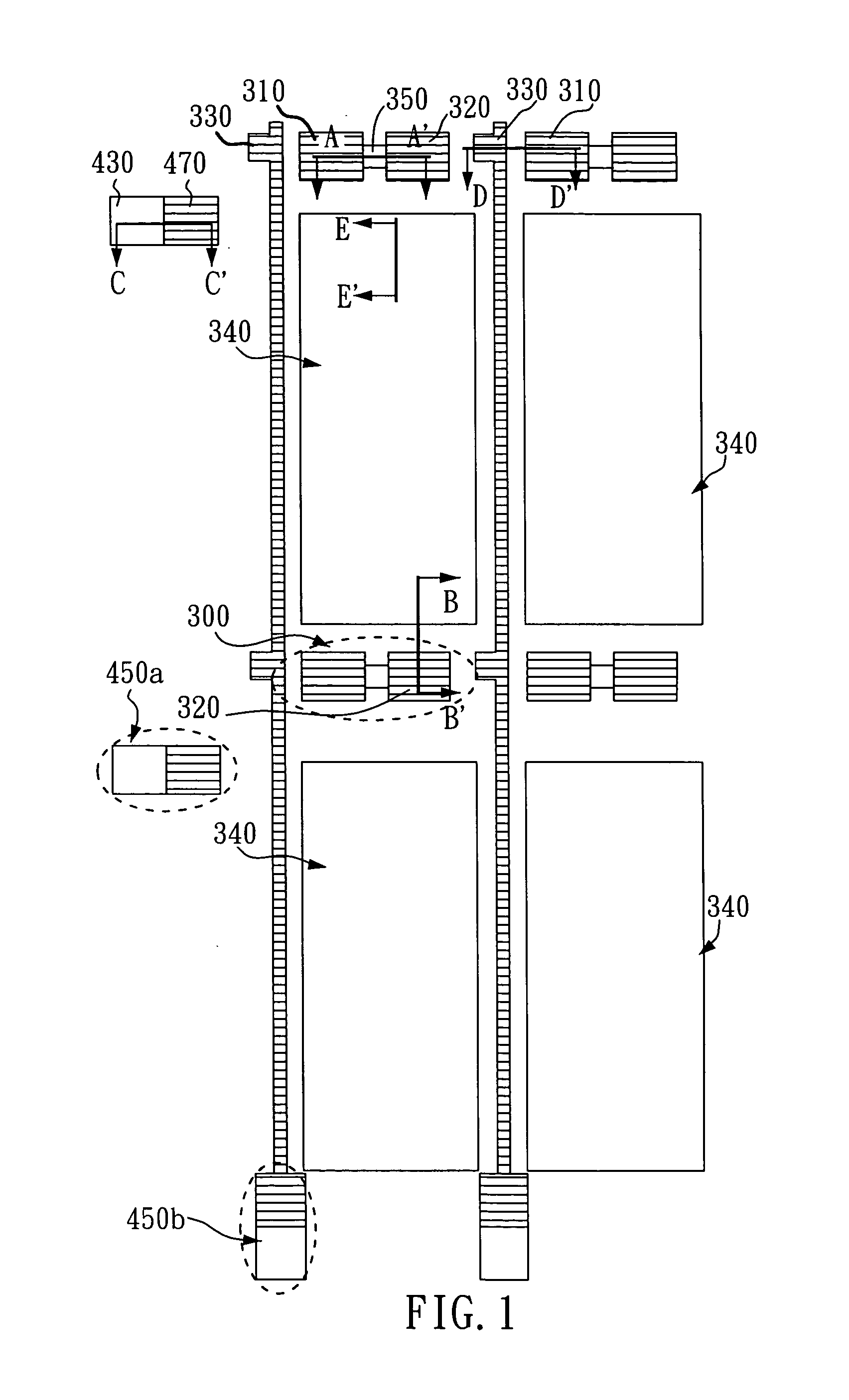
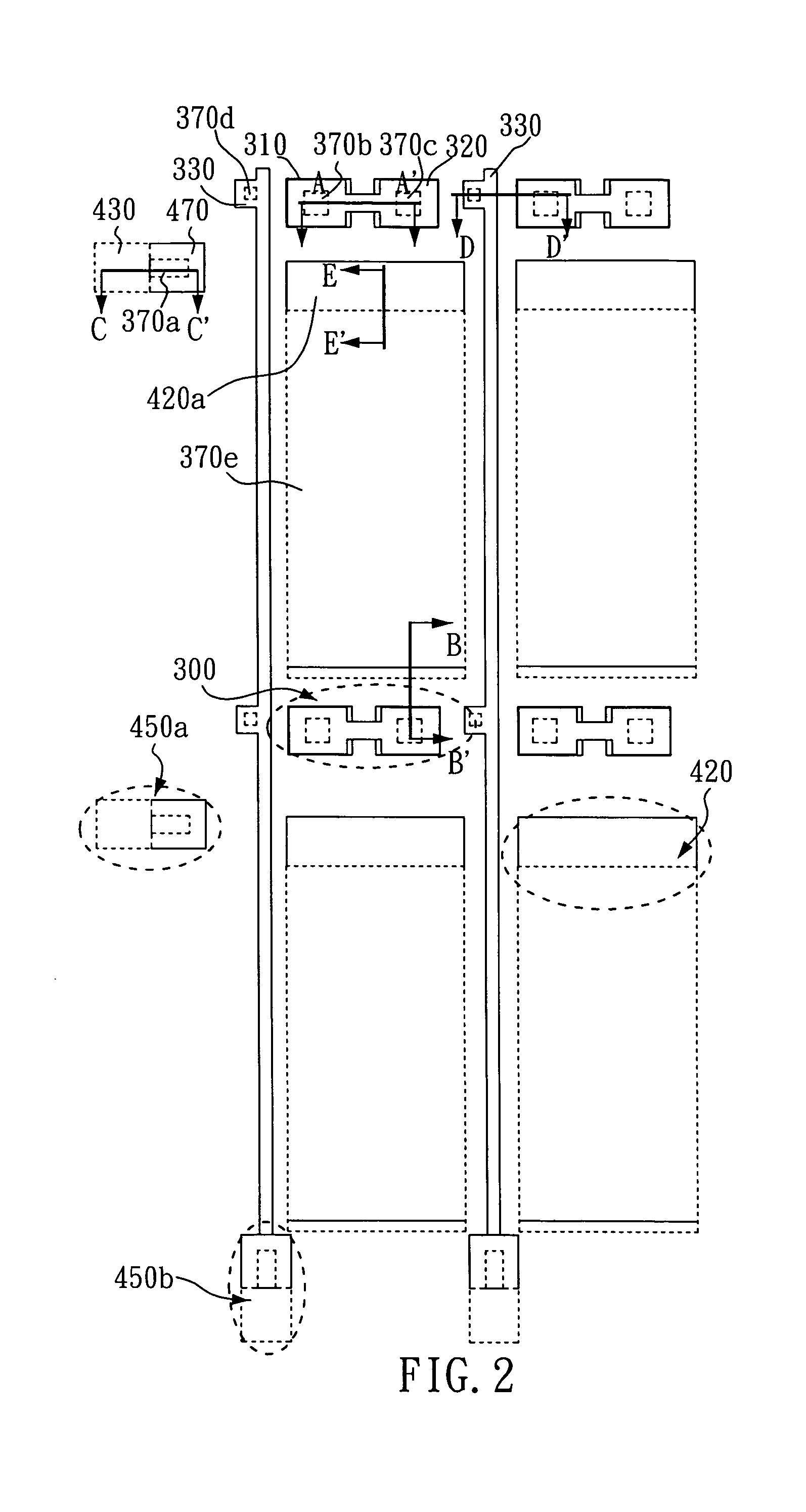
[0051] With reference to the bottom half part in FIG. 3, there is shown a thin film transistor area 300, a pixel electrode area 460, and a capacitor area 420 in every pixel area, which is surrounded by data signal lines 330 and scanning signal lines 380. In addition, a pattern of a peripheral circuit, the combination of the peripheral circuit area 450a with the peripheral circuit area 450b, is formed outside the pixel areas on the panel of the TFT LCD device. The data signal lines 330 and the scanning signal lines 380 are controlled by signals from an external driver respectively through the peripheral circuit area 450b and the peripheral circuit area 450a. In this embodiment, the structure of the peripheral circuit area 450a connected with the scanning signal lines 380 is as same as that of the peripheral circuit area 450b connected with the data signal lines 330, so the manufacturing flow of the peripheral circuit area 450b in the following description will be omitted. In the foll...


PUM


Abstract

A method for manufacturing a panel of a thin film transistor liquid crystal display device with three mask processes is disclosed. The method includes following steps: forming a transparent conductive layer, a first insulating layer, and a second metal layer on a transparent substrate in sequence; forming a source area, a drain area, a transparent electrode area, and data signal lines through a halftone photolithography and an etching; forming a semiconducting layer and a second insulating layer on the substrate in sequence; forming a semiconducting channel area in a thin film transistor area and contacts on the source area, the drain area, and the data signal lines through a photolithography and an etching; forming a third metal layer and a third insulating layer on the substrate in sequence; forming scanning signal lines and gate lines through a photolithography and an etching.

Description

BACKGROUND OF THE INVENTION [0001] 1. Field of the Invention [0002] The present invention relates to a method for manufacturing a panel of a thin film transistor liquid crystal display device and, more particularly, to a method for manufacturing a panel of a thin film transistor liquid crystal display device with three mask processes. [0003] 2. Description of Related Art [0004] Comparing with the cathode ray tube display, the liquid crystal display (LCD) has advantages on low power consumption, small occupied space, and free of irradiation. Depending on the liquid crystal operating principle, LCD device includes various specifications, which mainly classify to a passive matrix liquid crystal display (PM LCD) and a thin film transistor liquid crystal display (TFT LCD), wherein PM LCD further comprises twisted nematic (TN), super twisted nematic (STN), double layer twisted nematic (DSTN). The difference between these two specifications, the PM LCD and the TFT LCD, is about the orienta...

Claims


Application Information

Patent Timeline
IPC IPC(8): G02F1/1368G02F1/133G02F1/1343G02F1/1345G02F1/136G02F1/1362H01L21/336H01L21/77H01L27/12H01L29/786
CPCG02F1/13454G02F1/1362G02F1/136213H01L27/1288G02F2001/136236H01L27/1214G02F2001/136231G02F1/136231G02F1/136236H01L27/124
Inventor CHEN, HUNG-DE
Owner AU OPTRONICS CORP
Why Eureka
Try Eureka