

Semiconductor integrated circuit device including first, second and third gates
a technology of integrated circuits and semiconductors, applied in semiconductor devices, digital storage, instruments, etc., can solve the problems of increasing the word line voltage, reducing the operation speed, and affecting the operation speed, so as to achieve high operation speed and low defect density
- Summary
- Abstract
- Description
- Claims
- Application Information
AI Technical Summary
Benefits of technology
Problems solved by technology
Method used
Image

Examples
embodiment 1
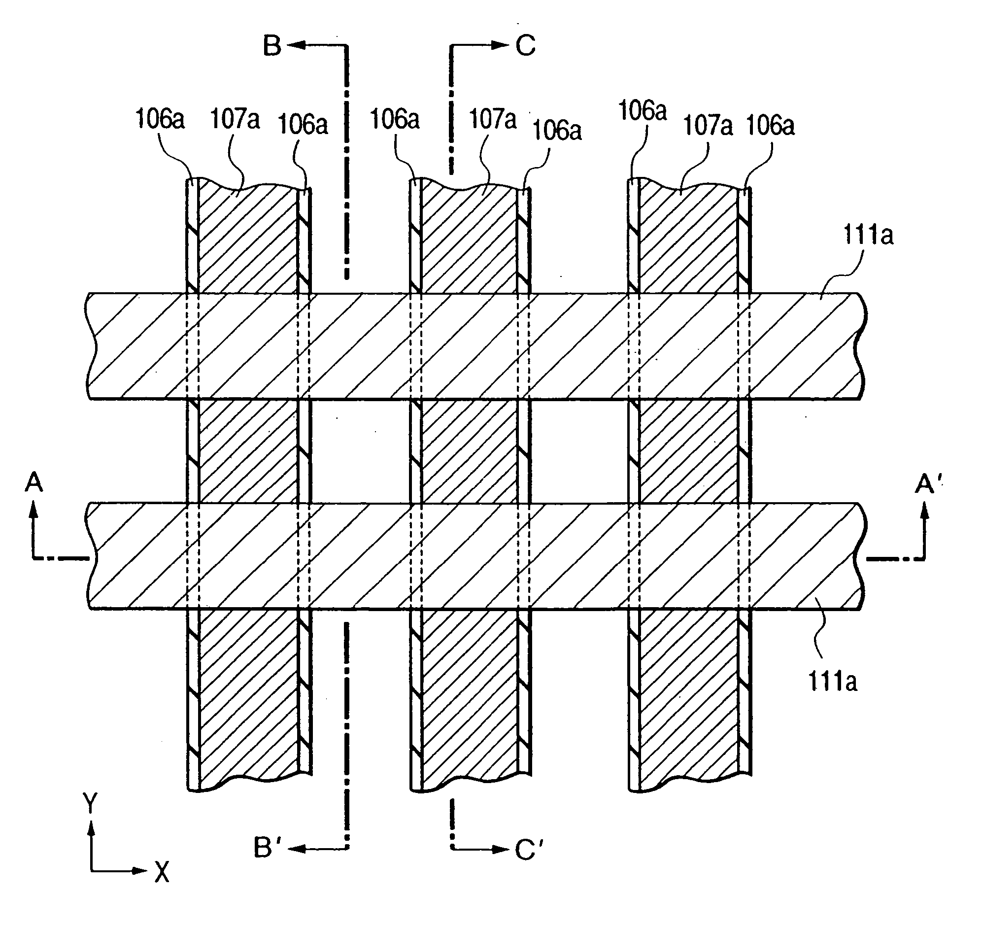
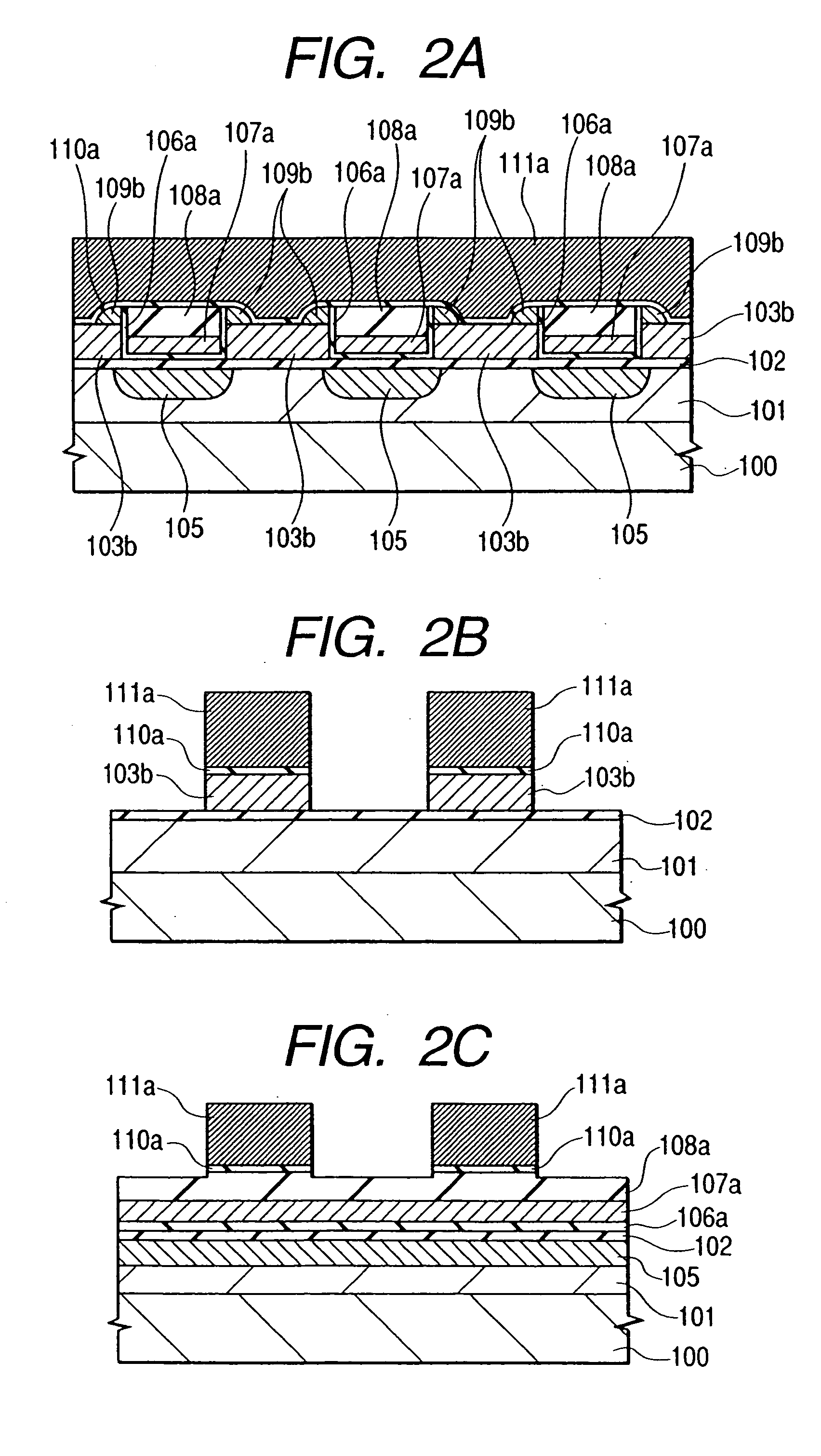
[0166]FIG. 1 is a partial plan view showing an example of the semiconductor integrated circuit device according to Embodiment 1 of the present invention. FIGS. 2A, 2B and 2C are sectional views taken along lines A-A′, B-B′ and C-C′ in FIG. 1, respectively. In the plan view of FIG. 1, hatching is applied to each member for ease of illustration and a part of members is omitted.
[0167] The semiconductor integrated circuit device of this embodiment has a memory cell of a so-called “flash memory”. The memory cell includes a source / drain 105 inside a well 101 formed on the main surface of a semiconductor substrate 100, a first gate (floating gate) 103b, a second gate (control gate) 111a and a third gate 107a. The control gate (second gate) 111a of each memory cell is connected to other in a row direction (x direction) and forms a word line WL.
[0168] The floating gate (first gate) 103b and the well 101 are isolated from each other by a gate insulator film (first insulator film) 102, and t...
embodiment 2
[0219]FIG. 16 is a sectional view showing an example of a semiconductor integrated circuit device according to Embodiment 2 of the present invention. The plan view of the semiconductor integrated circuit device of this embodiment is the same as FIG. 1 of the first embodiment. FIGS. 16A, 16B and 16C are sectional views taken along lines A-A′, B-B′ and C-C′ in FIG. 1, respectively.
[0220] The semiconductor integrated circuit device according to this embodiment is different from the semiconductor integrated circuit device of Embodiment 1 in only its source / drain diffusion layer 205. The materials of other members, their structures and arrangement, etc, are the same as those of Embodiment 1. Therefore, the explanation will be given on only the different portion, and the explanation of other members will be omitted.
[0221] The source / drain diffusion layer 205 is disposed vertically to the word line 111a and exists as a local source line and a local data line for connecting the source / dra...
embodiment 3
[0248]FIG. 22 is a partial plan view showing an example of the semiconductor integrated circuit device according to Embodiment 3 of the present invention, and FIGS. 23A, 23B and 23C are sectional views taken along lines A-A′, B-B′ and C-C′ in FIG. 22, respectively. Incidentally, each member is shown hatched with some members being omitted for ease of illustration in the plan view of FIG. 22. FIGS. 23A, 23B and 23C are sectional views taken along lines A-A′, B-B′ and C-C′ in FIG. 22, respectively.
[0249] The construction of the semiconductor integrated circuit device of this embodiment is substantially the same as that of Embodiment 2 with the exception that the film thickness of the insulator film 606a between the floating gate 103b and the third gate 107a is increased. The materials, constructions, arrangements, etc, of other members are substantially the same as those of Embodiment 2. Therefore, the explanation will be given on only the different portions and will be omitted on ot...
PUM
 Abstract
Description
Claims
Application Information