Electromagnetic wave shielding sheet
a shielding sheet and electromagnetic radiation technology, applied in the direction of identification means, instruments, transportation and packaging, etc., can solve the problems of affecting the accuracy of the width of the meshed structure, and the influence of the width accuracy, etc., to achieve excellent electromagnetic shielding ability, resist rusting, and satisfactory visibility of displayed images
- Summary
- Abstract
- Description
- Claims
- Application Information
AI Technical Summary
Benefits of technology
Problems solved by technology
Method used
Image
Examples
example 1
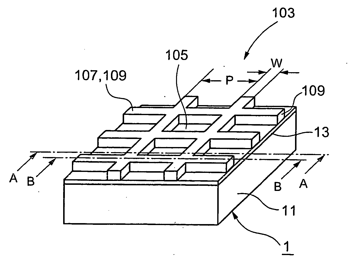
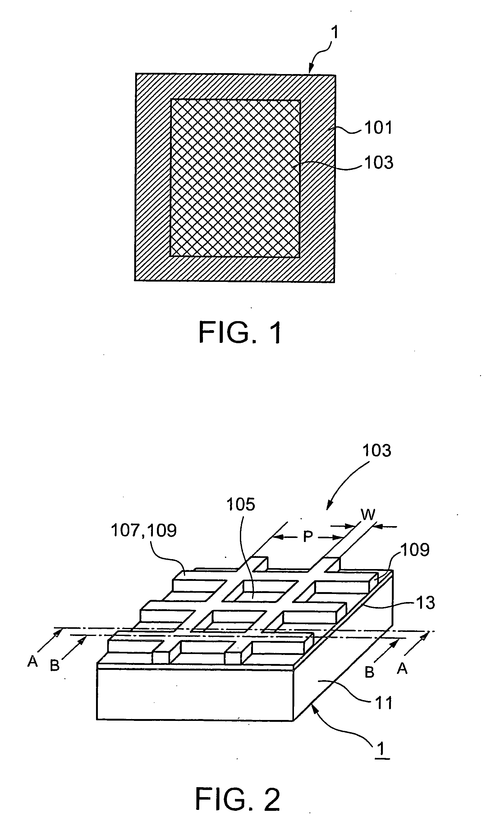
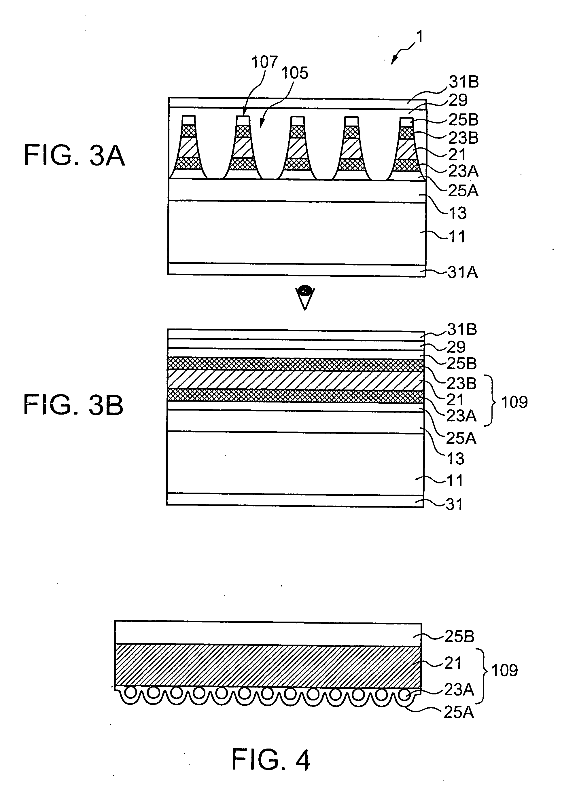
[0097] A conductive structure was formed by subjecting a 10 μm thick electrolytic Cu foil to a blackening process that forms a blackened layer consisting of Cu—Co alloy particles having a mean particle size of 0.3 μm and a chromating treatment that forms a chromated layer in that order. A 100 μm thick transparent, biaxially oriented PET film A4300® (Toyobo) as a base was laminated to the blackened layer of the Cu foil with a two-part polyurethane adhesive. A structure formed by laminating the PET film and the Cu foil was aged at 56° C. for four days. The two-part adhesive includes TAKERAKKU A-310® (polyol) (Takeda Yakuhin Kogyo) as an adhesive resin, and Hardener A-10® (isocyanate) (Takeda Yakuhin Kogyo) as a hardener. The two-part adhesive was spread in a 7 μm thick film in a dry state.
[0098] The structure formed in a continuous laminated film was masked and etched by a photolithographic process. The photolithographic process was carried out by a shadow mask manufacturing line for...
example 2
[0100] Electromagnetic shielding sheets in Example 2 were formed by the same method as that of forming the electromagnetic shielding sheets in Example 1, except that the former method used a ferric chloride solution having a Baume degree of 35° as an etchant.
example 3
[0102] Electromagnetic shielding sheets in Example 3 were fabricated by the steps of coating the surfaces of the meshed structures of the electromagnetic shielding sheets in Example 1 with a film of a flattening composition, laminating a 50 μm thick SP-PET20-BU® (Tosero), i.e., a PET film having a surface having a release characteristic, to the surface of the film of the flattening composition, exposing the thus coated electromagnetic shielding sheets to radiation of an intensity of 200 mj / cm2 (in terms of 365 nm) emitted by a high-pressure mercury lamp, and removing the SP-PET20-BU. The electromagnetic shielding sheets in Example 3 had a flattening layer of the flattening composition filling up the openings of the meshed structures.
[0103] The flattening composition was prepared by mixing 20 parts by mass of N-vinyl-2-pyrrolidone, 25 parts by mass dicyclopentenyl acrylate, 52 parts by mass oligoester acrylate (M-8060®, Toa Gosei), and 3 parts by mass 1-hydroxycyclohexyl phenylketon...
PUM
| Property | Measurement | Unit |
|---|---|---|
| width | aaaaa | aaaaa |
| widths | aaaaa | aaaaa |
| widths | aaaaa | aaaaa |
Abstract
Description
Claims
Application Information


