Superlattice nanopatterning of wires and complex patterns

Inactive Publication Date: 2005-11-10
CALIFORNIA INST OF TECH
View PDF4 Cites 23 Cited by
  • Summary
  • Abstract
  • Description
  • Claims
  • Application Information

AI Technical Summary

Benefits of technology

[0013] This technique to form nanometer scale features has several advantages over traditional approaches. First, the difficulty of defining nanometer scale patterns using photolithography due to the fundamental physical properties of light and electron beams are completely avoided, as there is little problem producing superlattices with arbitrary thick (or thin) layers and periodicity. In addition, the extremely expensive fabrication facilities required for nanometer photolithography are not needed, as the precise positioning tools and special optics required for photolithography at these scales are obviated. Second, unlike e-beam lithography or ion-milling, the superlattice approach is not serial, and can be performed repeatedly to form complex patterns. For mass production purposes, the superlattice process can be applied to form a ‘master,’ in another material if desired (for additional toughness for instance), to template very complicated structures in one step. Third, the superlattice technique can be used to directly deposit fully formed metallic wires, without the lift-off processing steps used in both photo- and e-beam lithography. This is an important advantage, as complete removal of excess metal in the lift-off step is a very challenging for nanometer features, often causing complete loss of the device and lowering overall yields.

Problems solved by technology

However, because of a combination of physical and economic reasons, the miniaturization that has accompanied the growth of Si IC's is reaching its limit.
The major problem with (1) is the capital expense necessary to build equipment capable of fabricating devices on the nanometer lengthscale.
The properties of light at these length scales require expensive optical components, as well as precision translation stages and alignment equipment.
Indeed, some components necessary to produce 30 nm photolithographic structures have not even been invented yet.
Writing a wafer full of complex devices, each containing trillions of components, could well require many years.
While very small structures (wires and discs), with a smallest dimension of 10 to 20 nanometers, can be patterned using various of the above techniques, it is very difficult to fabricate such small structures at a high density.
The subsequent processing steps, such as polymer removal, pattern etching, and metal deposition are very difficult to control at nanoscale dimensions, and so it is very difficult to transfer the atomic-level control that is realized in the superlattice structure into the final pattern of nanostructures.

Method used


Image

  • Superlattice nanopatterning of wires and complex patterns
  • Superlattice nanopatterning of wires and complex patterns
  • Superlattice nanopatterning of wires and complex patterns

Examples


Embodiment Construction

Definitions

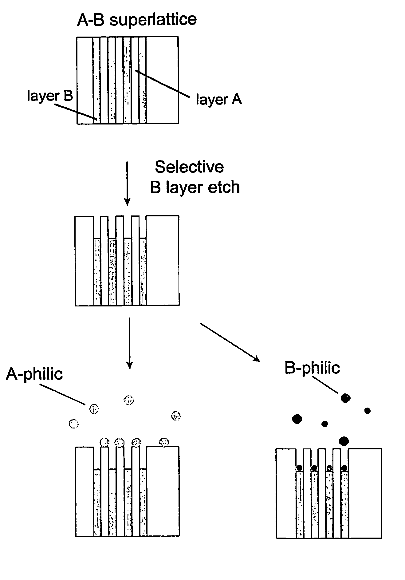
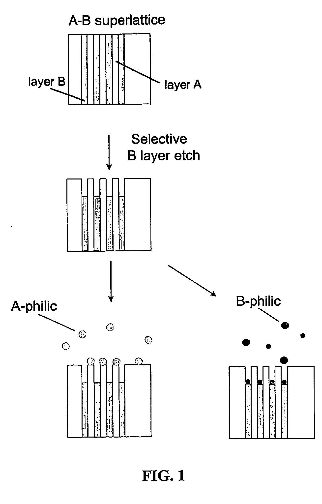
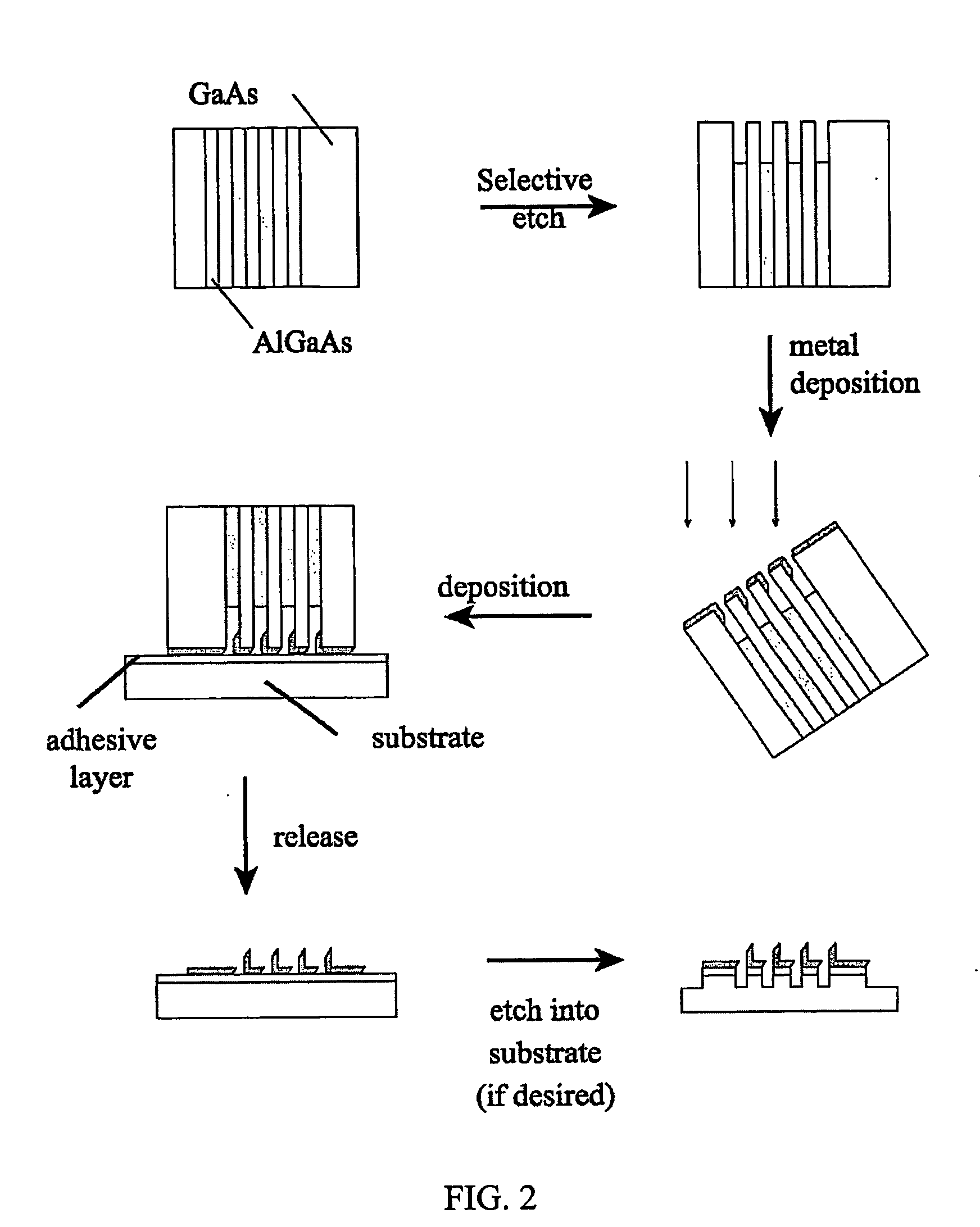
[0031] A ‘superlattice’ is defined as a stack of alternating layers of non-identical materials. This includes, but is not exclusive to, semiconductors, metals, insulators, organic and ceramics. The superlattice may have several different types or composition of layers, with a minimum of two.

[0032] A ‘master’ is a pattern or template that is used repeatedly to pattern other surfaces. A rubber stamp is an example of a master, used to repeatedly transfer an ink pattern to a paper substrate.

[0033] Thicknesses of GaAs / AlxGa1-xAs (0.5<x<1) layers are labeled as xx / yy nm, denoting xx nm wide GaAs layers alternating with yy nm wide AlGaAs layers. The same notation will be used for the width of the deposited wires and the spaces in between. Thus, 10 / 20 nm Pt wires denotes 10 nm wide Pt wires with 20 nm space between each wire, for a total center-to-center distance of 30 nm. The ‘pitch’ of a set of wires is then defined as the center-to-center distance of each wire.

Superlatti...


PUM

PropertyMeasurementUnit
Widthaaaaaaaaaa
Widthaaaaaaaaaa
Widthaaaaaaaaaa

Abstract

Fabrication of metallic or non-metallic wires with nanometer widths and nanometer separation distances without the use of lithography. Wires are created in a two-step process involving forming the wires at the desired dimensions and transferring them to a planar substrate. The dimensions and separation of the wires are determined by the thicknesses of alternating layers of different materials that are in the form of a superlattice. Wires are created by evaporating the desired material onto the superlattice that has been selectively etched to provide height contrast between layers. The wires thus formed upon one set of superlattice layers are then transferred to a substrate.

Description

STATEMENT REGARDING FEDERALLY SPONSORED RESEARCH OR DEVELOPMENT [0001] This invention was made with support from the Defense Advanced Research Projects Agency (DARPA) Grant #MDA972-01-3-0005. The government has certain rights in this invention.BACKGROUND OF THE INVENTION [0002] 1. Field of the Invention [0003] The present invention involves the production of electronic and mechanical devices with length scales measured in nanometers to microns. More particularly, the invention encompasses complicated electrical circuits, mechanical devices, and spatially modulated physical properties. Currently, similar devices (with larger feature sizes) are fabricated using photolithography and related processes often employed by the semiconductor industry. [0004] 2. Description of Related Art [0005] The silicon integrated circuit industry (IC) has dominated electronics and has helped it grow to become one of the world's largest and most critical industries over the past thirty-five years. However...

Claims


Application Information

Patent Timeline
IPC IPC(8): B29C33/00B32B5/02G03F7/00H01LH01L21/033H01L21/768H01L21/8238
CPCB82Y10/00B82Y30/00B82Y40/00G03F7/0002H01L21/0337Y10S977/76H01L21/76838Y10S977/755Y10S977/762Y10S977/847Y10S977/938H01L21/76802
Inventor HEATH, JAMES R.PETROFF, PIERRE M.MELOSH, NICHOLAS A.
Owner CALIFORNIA INST OF TECH
Why Eureka
Try Eureka