
Method of cleaning an interior of a remote plasma generating tube and appartus and method for processing a substrate using the same

a plasma generating tube and interior cleaning technology, applied in the direction of conveyor parts, chemistry apparatus and processes, transportation and packaging, etc., can solve the problems of poor reliability and response speed of semiconductor devices, failure of multi-layer structures of semiconductor devices, and native oxide film may not be easily removed by wet etching processes, so as to achieve effective removal, prevent contamination of semiconductor substrates, and improve the effect of a semiconductor device manufacturing process

Inactive Publication Date: 2005-11-24
ULVAC INC +1
View PDF18 Cites 92 Cited by
  • Summary
  • Abstract
  • Description
  • Claims
  • Application Information

AI Technical Summary

Benefits of technology

[0017] It is a feature of an embodiment of the present invention to provide a method of cleaning a remote plasma generating tube to remove various particles from an interior of the remote plasma generating tube using cleaning plasma, thereby preventing contamination of semiconductor substrates being processed.
[0018] It is another feature of an embodiment of the present invention to provide a method of processing a substrate using a remote plasma generating tube that reduces contamination without reducing throughput of the process.
[0019] It is still another feature of an embodiment of the present invention to provide an apparatus for processing a substrate using a remote plasma generating tube that is able to prevent contamination of a substrate being processed therein.
[0045] According to the various embodiments of the present invention, particles generated on an interior of a remote plasma generating tube may be effectively removed using cleaning plasma. Therefore, contamination of semiconductor substrates may be prevented during an etching of predetermined layers formed on the semiconductor substrates. In addition, productivity of a process for manufacturing semiconductor devices may be improved. When a batch-type substrate processing apparatus is employed, the interior of the remote plasma generating tube may be cleaned between loading and unloading of the semiconductor substrates into or out of a processing chamber so that the semiconductor substrates may be more efficiently processed without decreasing throughput of the batch-type substrate processing apparatus.

Problems solved by technology

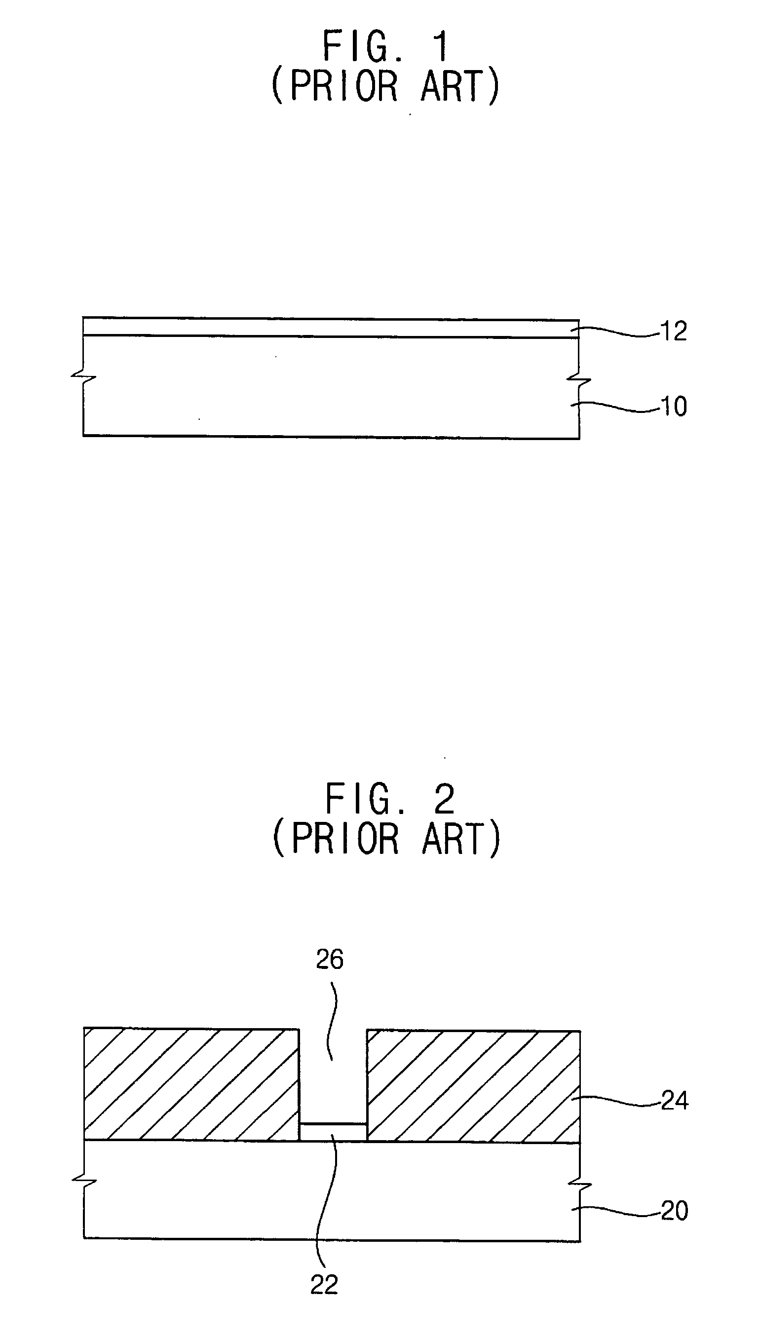
The native oxide film 12 may cause a failure of a semiconductor device having the multi-layered structure.
In addition, the native oxide film 12 may increase the contact resistance of the semiconductor device so that the semiconductor device may have poor reliability and response speed.
However, the native oxide film may not be easily removed by the wet etching process when the native oxide film is positioned in a contact hole having a high aspect ratio.
Further, a chemical used in the wet etching process may damage other layers or wirings formed on the substrate.
The excited remote plasma, however, may cause particles to attach to an interior of the remote plasma generating tube.
When the particles become detached and are introduced into the processing chamber, semiconductor substrates in the processing chamber may be contaminated by the particles.
As a result, semiconductor devices may perform poorly and exhibit poor reliability due to the particles.

Method used


Image

  • Method of cleaning an interior of a remote plasma generating tube and appartus and method for processing a substrate using the same
  • Method of cleaning an interior of a remote plasma generating tube and appartus and method for processing a substrate using the same
  • Method of cleaning an interior of a remote plasma generating tube and appartus and method for processing a substrate using the same

Examples


Embodiment Construction

[0057] Korean Patent Application No. 2004-36416, filed on May 21, 2004, in the Korean Intellectual Property Office, and entitled: “Method of Cleaning a Surface of a Remote Plasma Generating Tube and Apparatus and Method for Processing a Substrate Using the Same,” is incorporated by reference herein in its entirety.

[0058] The present invention will now be described more fully hereinafter with reference to the accompanying drawings, in which exemplary embodiments of the invention are shown. The invention may, however, be embodied in different forms and should not be construed as limited to the embodiments set forth herein. Rather, these embodiments are provided so that this disclosure will be thorough and complete, and will fully convey the scope of the invention to those skilled in the art. Like reference numerals refer to like elements throughout.

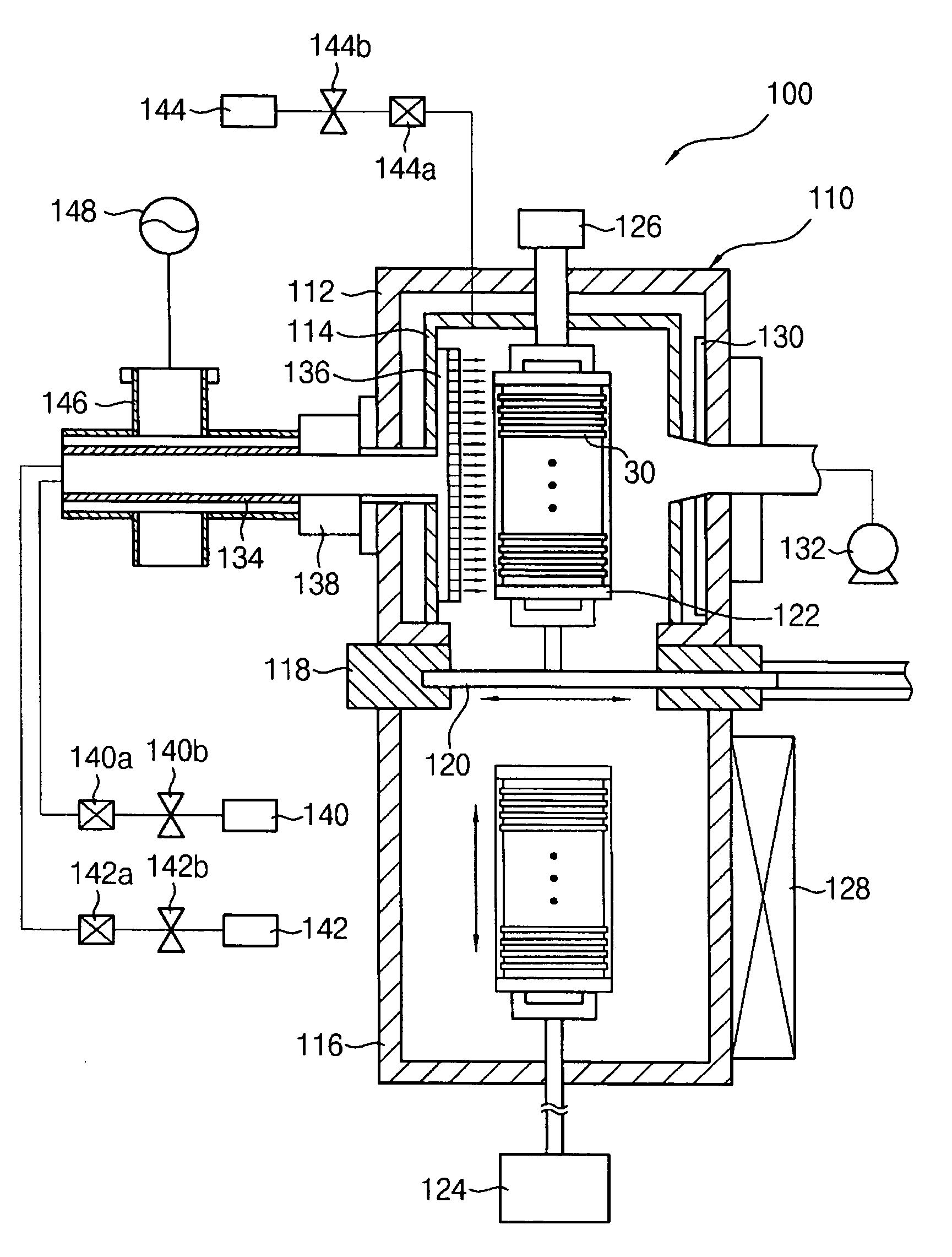
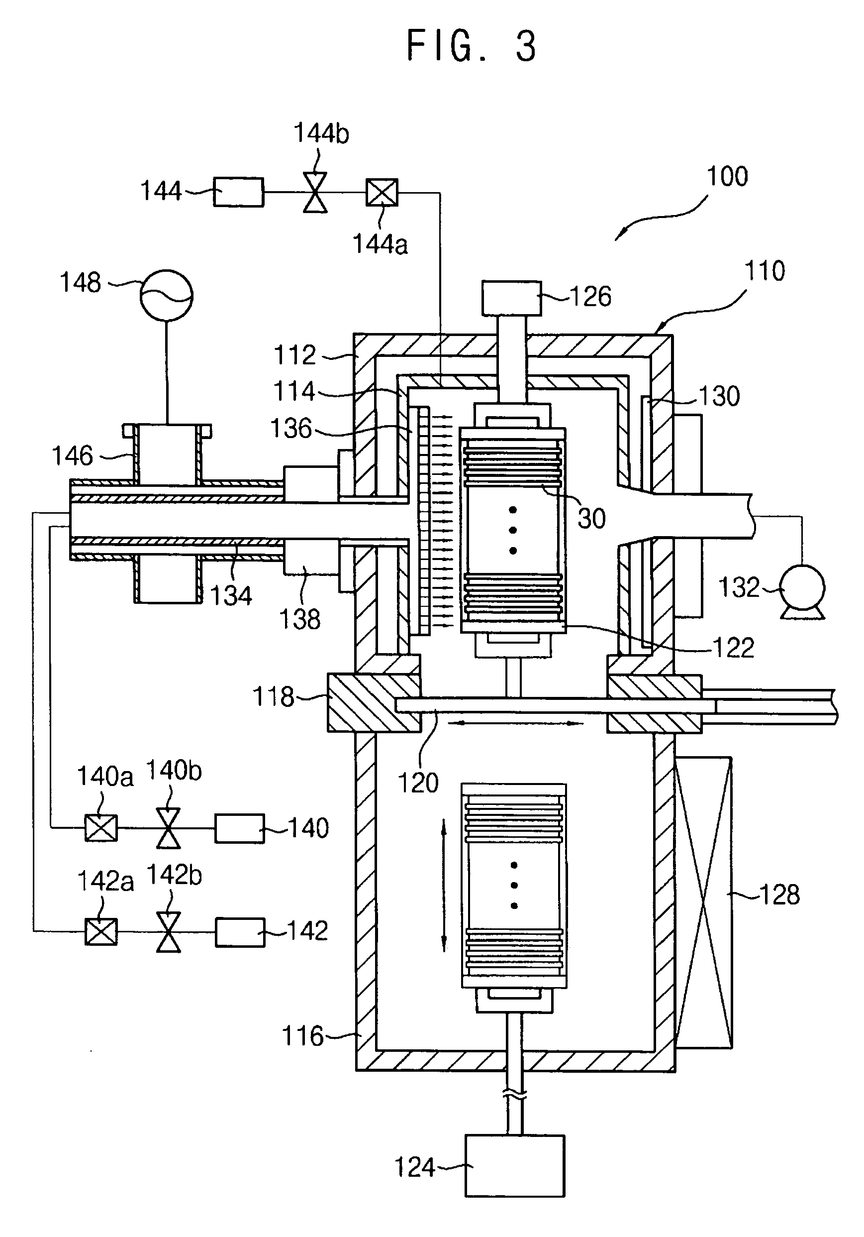
[0059]FIG. 3 illustrates a cross-sectional view of an apparatus having a remote plasma generating tube for processing a substrate accord...


PUM

PropertyMeasurementUnit
Temperatureaaaaaaaaaa
Timeaaaaaaaaaa

Abstract

A method of cleaning a remote plasma generating tube, and an apparatus and method for processing a substrate using the same, includes providing a cleaning gas into the remote plasma generating tube for generating a remote plasma, the remote plasma generating tube being connected to a processing chamber for processing a substrate using the remote plasma, forming a cleaning plasma from the cleaning gas, and removing particles formed inside the remote plasma generating tube using the cleaning plasma.

Description

BACKGROUND OF THE INVENTION [0001] 1. Field of the Invention [0002] The present invention relates to an apparatus and a method for processing a semiconductor substrate. More particularly, the present invention relates to a method of cleaning an interior of a remote plasma generating tube, and a method and an apparatus for processing a semiconductor substrate using the same. [0003] 2. Description of the Related Art [0004] Generally, semiconductor devices are manufactured by performing a fabrication process in which electrical circuits are formed on a silicon wafer, and an electrical die sorting (EDS) process in which the electrical characteristics of the electrical circuits formed by the fabrication process are inspected. Additionally, the semiconductor devices are independently encapsulated using an epoxy resin in a packaging process. [0005] A semiconductor device, such as a DRAM of 256 mega bits or an SRAM of giga bits, typically has a multi-layered structure. In a conventional sem...

Claims


Application Information

Patent Timeline
IPC IPC(8): B44C1/22H01L21/3065H01J37/32H01J37/34H01L21/304H01L21/677H01L21/68
CPCH01J37/32192H01J37/32357H01L21/67069H01J37/32862H01J37/32449H01L21/304
Inventor PARK, JAE-YOUNGLEE, SEUNG-JINKIM, YOUNG-MIN
Owner ULVAC INC
Learn More