

Plasma processing apparatus
a technology of processing apparatus and plasma, which is applied in the direction of plasma technique, chemical vapor deposition coating, coating, etc., can solve the problems of difficult to carry out plasma treatment over a large area substrate, serious problems, etc., and achieve the effect of improving the uniformity of generating plasma
- Summary
- Abstract
- Description
- Claims
- Application Information
AI Technical Summary
Benefits of technology
Problems solved by technology
Method used
Image

Examples
first embodiment
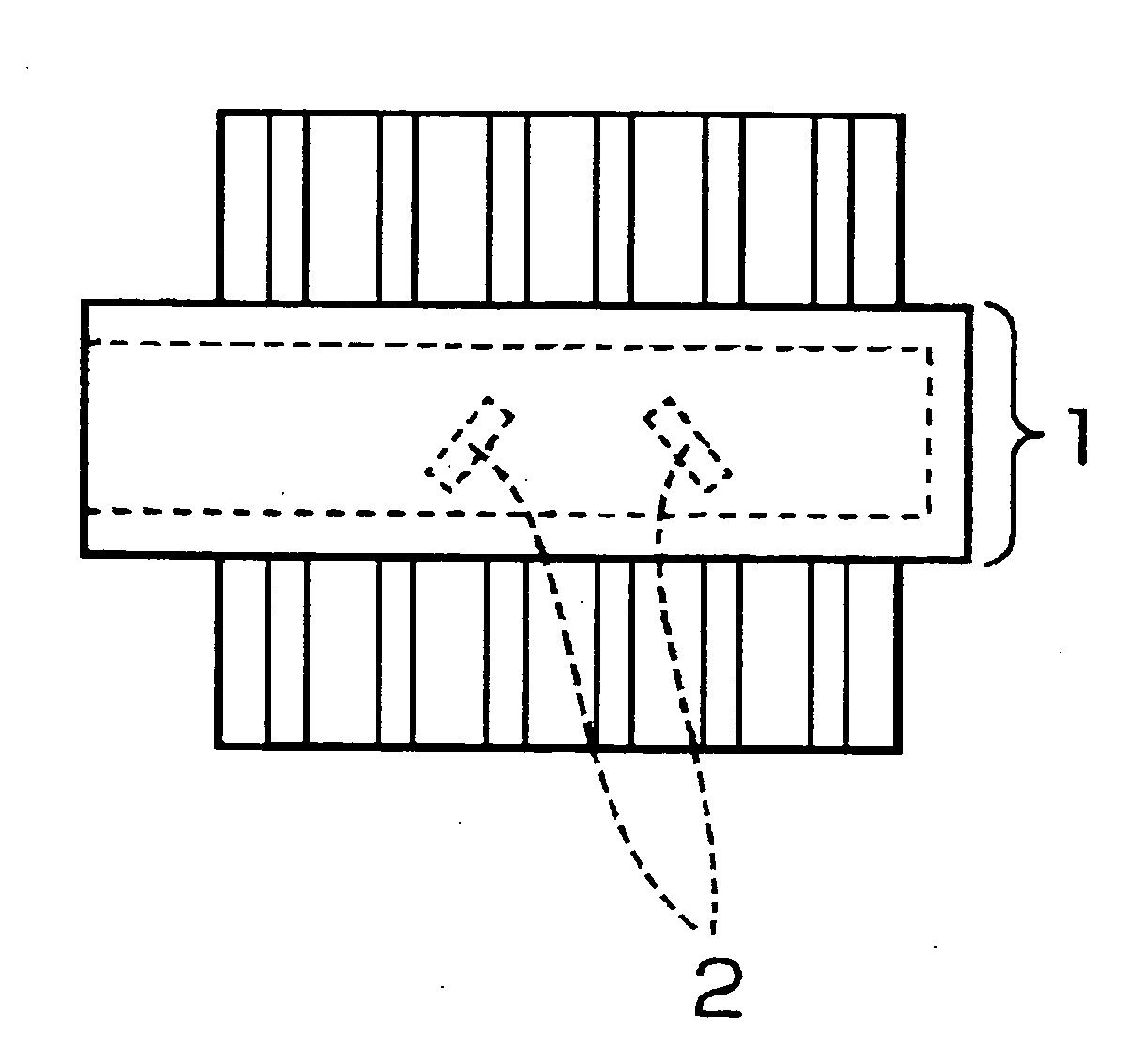
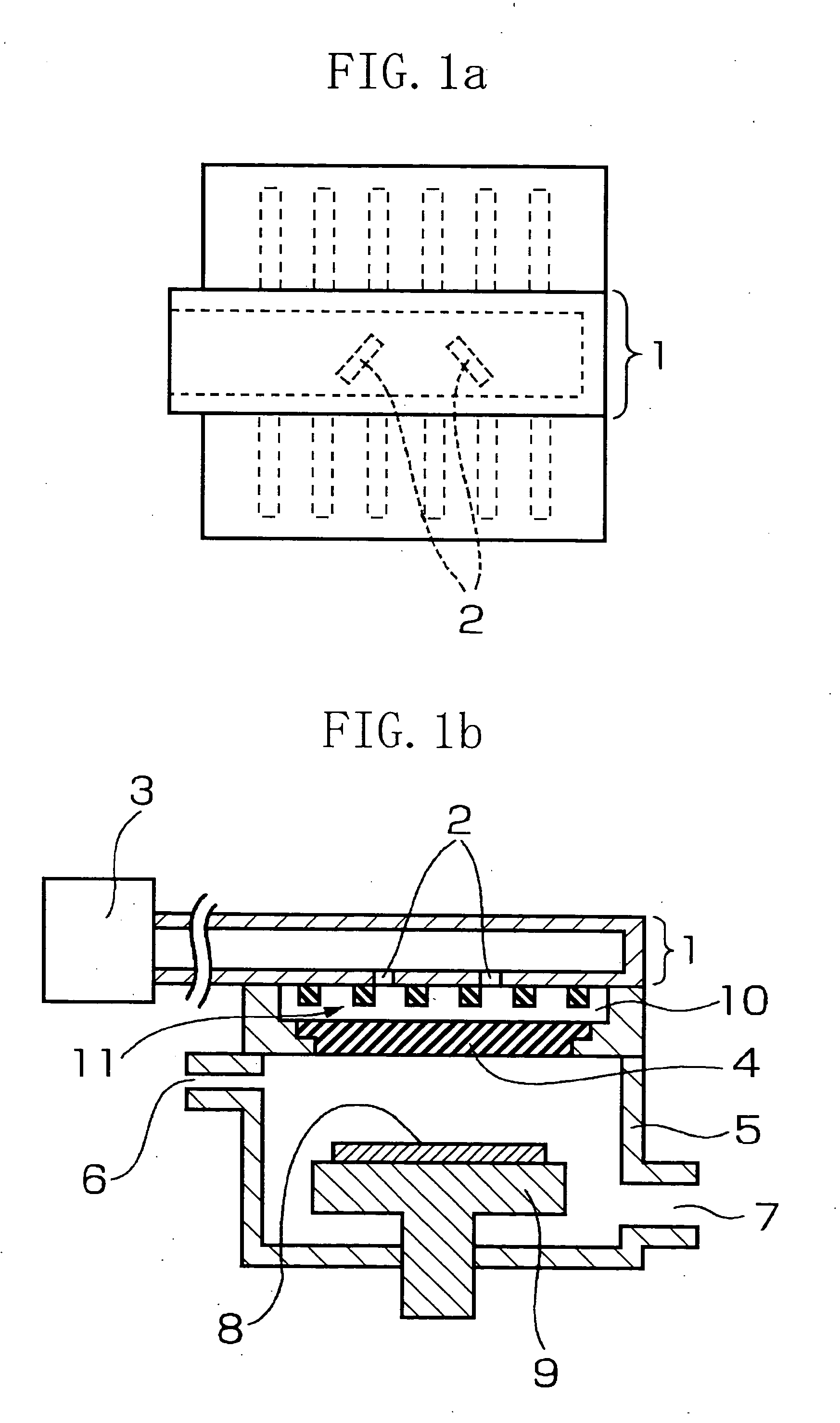
[0060]FIG. 1(a) is a top view of the first embodiment of the plasma treatment apparatus according to the invention while FIG. 1(b) is a sectional view of the same.
[0061] Referring to FIGS. 1(a) and 1(b), a reference numeral 1 indicates a rectangular waveguide; 2 a waveguide antenna; 3 an electromagnetic wave source for instance a microwave source; 4 an electromagnetic wave radiation window (electromagnetic wave introduction window) made up of a dielectric such as quartz, glass, ceramics and so on; 5 a vacuum container; 6 a gas introduction system; 7 a gas exhaust system; 8 a substrate subject to plasma treatment; 9 a substrate mount portion; 10 a dielectric space (air space) sandwiched between the waveguide antenna 2 and the electromagnetic wave window 4; and 11 an uneven portion provided so as to oppose to the electromagnetic wave radiation window 4 of the waveguide 1.
[0062] The vacuum container 5 in which the plasma is generated, is connected with the gas introduction system 6 f...
second embodiment
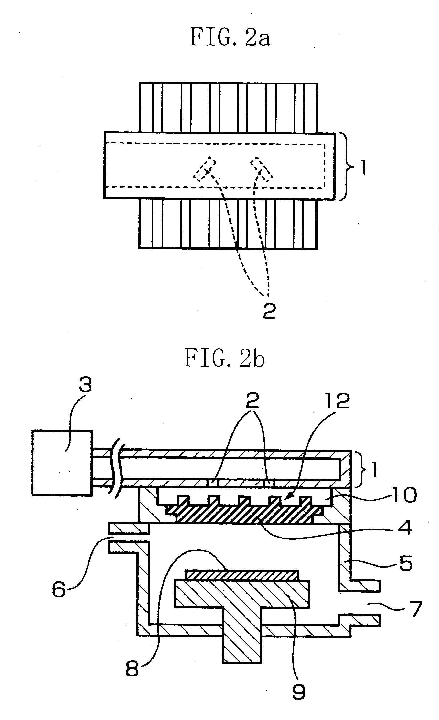
[0071]FIG. 2(a) is a top view of the second embodiment of the plasma treatment apparatus according to the invention while FIG. 2(b) is a sectional view of the same.
[0072] In FIGS. 2(a) and 2(b), a reference numeral 12 indicates an uneven portion which is provided on the surface of the electromagnetic wave radiation window 4 opposite to the waveguide 1.
[0073] In the second embodiment, a plurality of thin elongated projection portions having a width of 10 mm and a height of 5 mm are aligned at an interval of 30 mm on the surface of the electromagnetic wave radiation window 4 opposing to the waveguide 1. With this, an uneven portion 12 is constituted.
[0074] The projection portion of the uneven portion 12 of the electromagnetic wave radiation window 4 is set up at a distance of 5 mm from the outside surface of the waveguide 1 on which the waveguide antenna 2 is provided. The other surface of the electromagnetic wave radiation window 4 having no uneven portion 12 but coming in contact...
third embodiment
[0079]FIG. 3(a) is a top view of the second embodiment of the plasma treatment apparatus according to the invention while FIG. 3(b) is a sectional view of the same.
[0080] In FIGS. 3(a) and 3(b), a reference numeral 13 indicates a glass plate constituting an electromagnetic wave radiation window 4 and 14 a mixing member made of spherical ceramics mixed to the glass plate 13.
[0081] In the third embodiment, the electromagnetic wave radiation window 4 is made of the glass plate (dielectric constant: 4.7) 13 mixed with the mixing member 14 such as ceramics for instance alumina (dielectric constant: 9) and so on.
[0082] For instance the diameter of the spherical mixing member 14 is 2.5 cm while the thickness of the electromagnetic wave radiation window 4 is 5 cm. The diameter of the mixing member 14 is made larger than ⅛ of the wavelength of the microwave. With this, it becomes possible to efficiently disperse the microwave by reflecting and scattering it. Like this, if there is used th...
PUM
| Property | Measurement | Unit |
|---|---|---|
| diameter | aaaaa | aaaaa |
| height | aaaaa | aaaaa |
| height | aaaaa | aaaaa |
Abstract
Description
Claims
Application Information