Nitride-based semiconductor element and method of forming nitride-based semiconductor

a technology of nitride-based semiconductor and semiconductor elements, which is applied in the direction of semiconductor lasers, semiconductor laser structural details, lasers, etc., can solve the disadvantageous increase of the etching time for bringing the substrate b>101/b> into the ridged shape, deterioration of the element characteristics of the semiconductor element, etc., and achieve excellent element characteristics and superior mass productivity.

Inactive Publication Date: 2005-12-01
EPISTAR CORP
View PDF12 Cites 44 Cited by
  • Summary
  • Abstract
  • Description
  • Claims
  • Application Information

AI Technical Summary

Benefits of technology

[0014] An object of the present invention is to provide a nitride-based semiconductor element having superior mass productivity and excellent element characteristics.

Problems solved by technology

Such dislocations in the nitride-based semiconductor layer result in deterioration of the element characteristics of the semiconductor element and reduction of the reliability thereof.
Thus, the etching time for bringing the substrate 101 into the ridged shape is disadvantageously increased.
Consequently, the nitride-based semiconductor is disadvantageously reduced in mass productivity.

Method used


Image

  • Nitride-based semiconductor element and method of forming nitride-based semiconductor
  • Nitride-based semiconductor element and method of forming nitride-based semiconductor
  • Nitride-based semiconductor element and method of forming nitride-based semiconductor

Examples


first embodiment

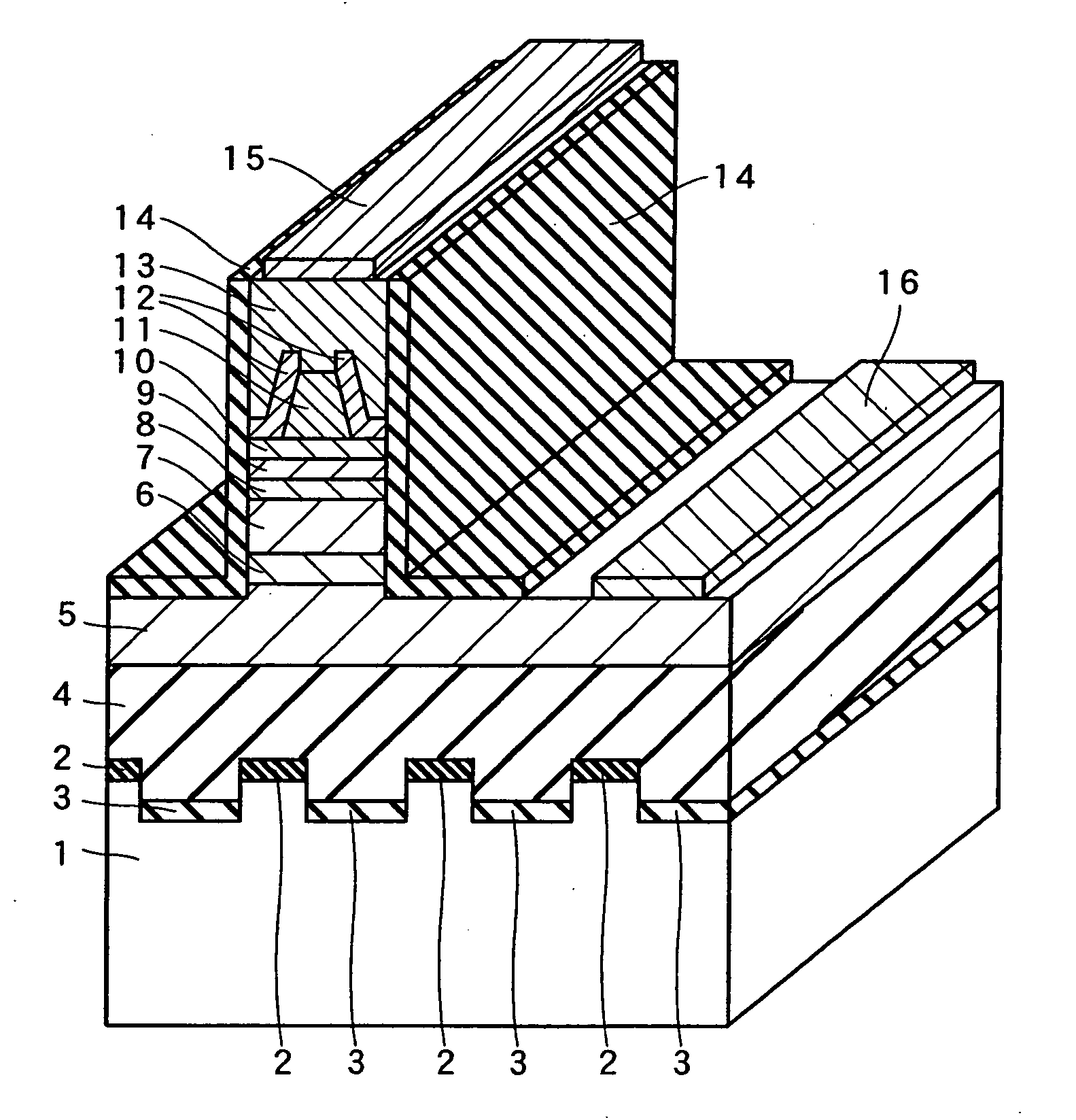
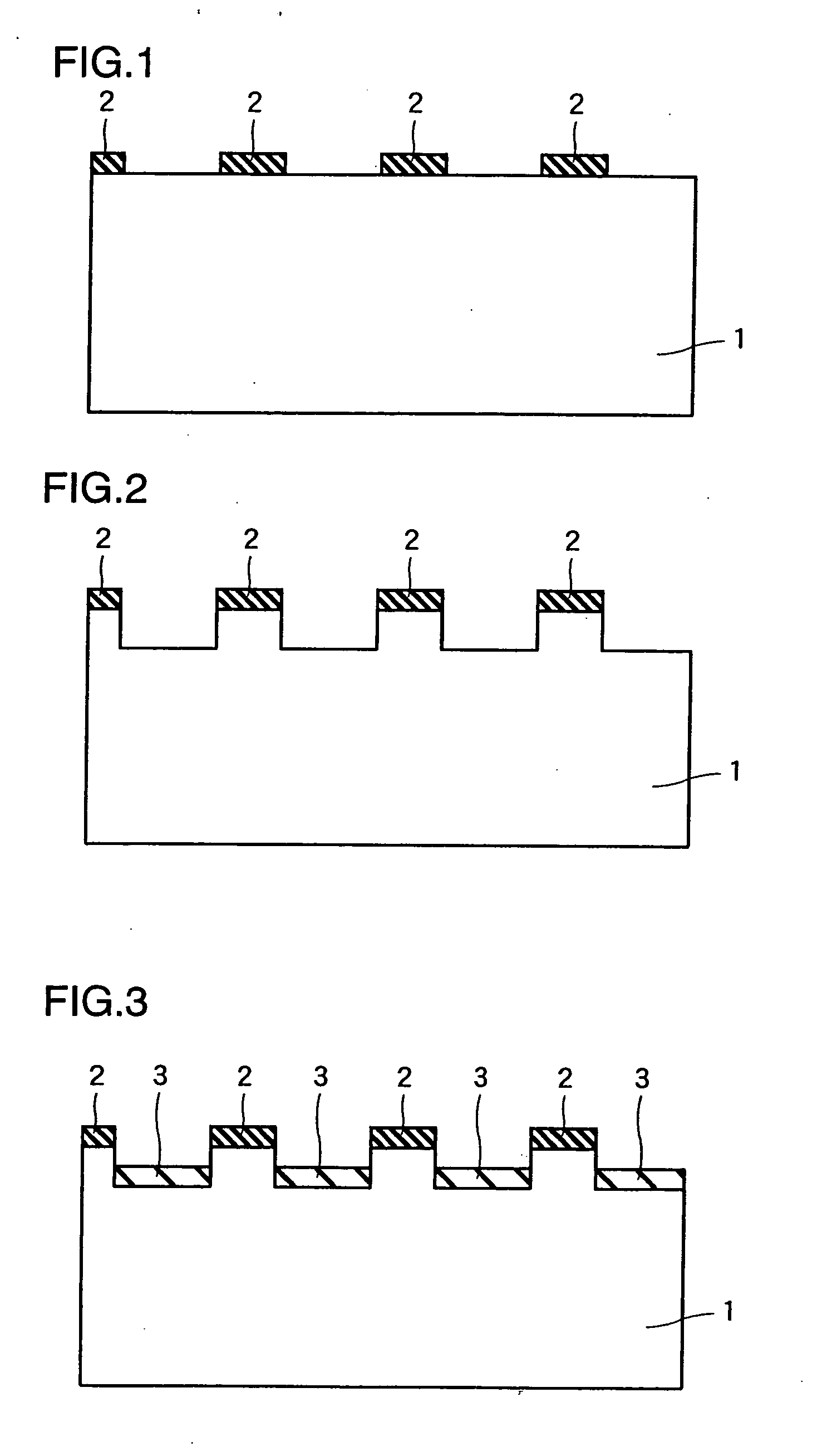
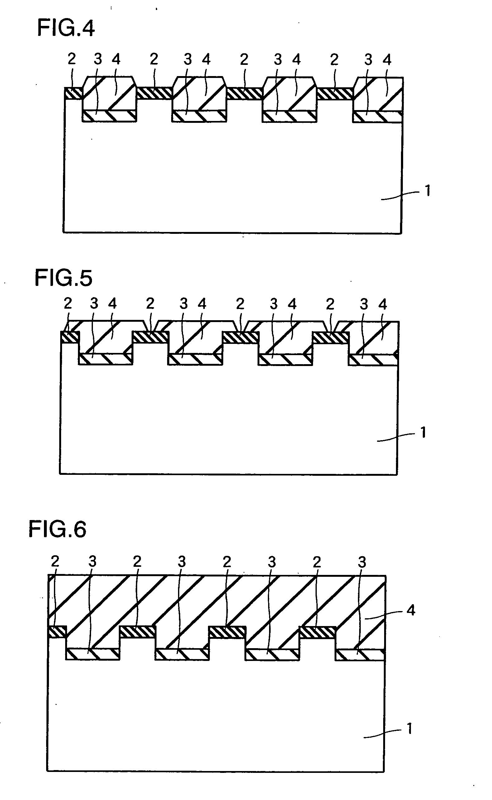
[0049] A method of forming a nitride-based semiconductor according to a first embodiment of the present invention is described with reference to FIGS. 1 to 6.

[0050] First, striped mask layers 2 of SiO2 having a thickness of about 0.5 μm are formed on a sapphire (0001) plane substrate 1 (hereinafter referred to as “sapphire substrate 1”), as shown in FIG. 1. The stripe patterns of the mask layers 2 are formed in a cycle of about 7 μm so that the width of the mask layers 2 is about 5 μm and the interval between each adjacent pair of mask layers 2 (the width of mask openings) is about 2 μm. The striped mask layers 2 are formed in parallel to the [1-100] direction of the sapphire substrate 1. The sapphire substrate 1 is an example of the “substrate” according to the present invention.

[0051] The mask layers 2 are employed as masks for etching the surface of the sapphire substrate 1 by a thickness of about 1 μm through RIE (reactive ion etching) or the like. Thus, the surface of the sap...

second embodiment

[0066] Referring to FIGS. 8 to 13, an n-type Si (111) plane substrate 21 (hereinafter referred to as “Si substrate 21”) having conductivity is employed in a second embodiment of the present invention in place of the insulating sapphire substrate 1 in the first embodiment. A method of forming a nitride-based semiconductor according to the second embodiment is now described with reference to FIGS. 8 to 13.

[0067] According to the second embodiment, striped mask layers 22 of SiO2 having a thickness of about 0.5 μm are formed on the n-type Si substrate 21, as shown in FIG. 8. The stripe patterns of the mask layers 22 are formed in a cycle of about 7 μm, so that the mask layers 22 are about 5 μm in width and the interval between each adjacent pair of mask layers 22 (the width of mask openings) is about 2 μm. The striped mask layers 22 are formed in parallel to the [1-10] direction of the Si substrate 21. The Si substrate 21 is an example of the “substrate” according to the present invent...

third embodiment

[0084] Referring to FIGS. 15 to 20, epitaxial lateral overgrowth is performed through an underlayer 43 comprising a surface having projection portions formed on a sapphire (0001) plane substrate 41 (hereinafter referred to as “sapphire substrate 41”) in a third embodiment of the present invention. A method of forming a nitride semiconductor according to the third embodiment is now described in detail with reference to FIGS. 15 to 20.

[0085] First, low-temperature buffer layers 42 of AlGaN having a thickness of about 15 nm and the underlayer 43 of undoped GaN having a thickness of about 2 μm are formed on the sapphire substrate 41 by a crystal growth method such as MOVPE, as shown in FIG. 15. The sapphire substrate 41 is an example of the “substrate” according to the present invention. The low-temperature buffer layers 42 are examples of the “buffer layer” according to the present invention.

[0086] Striped mask layers 44 of SiO2 having a thickness of about 0.5 μm are formed on the un...


PUM


Abstract

A nitride-based semiconductor element having superior mass productivity and excellent element characteristics is obtained. This nitride-based semiconductor element comprises a substrate comprising a surface having projection portions, a mask layer formed to be in contact with only the projection portions of the surface of the substrate, a first nitride-based semiconductor layer formed on recess portions of the substrate and the mask layer and a nitride-based semiconductor element layer, formed on the first nitride-based semiconductor layer, having an element region. Thus, the first nitride-based semiconductor layer having low dislocation density is readily formed on the projection portions of the substrate and the mask layer through the mask layer serving for selective growth. When the nitride-based semiconductor element layer having the element region is grown on the first nitride-based semiconductor layer having low dislocation density, a nitride-based semiconductor element having excellent element characteristics can be readily obtained. The first nitride-based semiconductor layer is formed through only single growth on the substrate, whereby a nitride-based semiconductor element having excellent mass productivity is obtained.

Description

BACKGROUND OF THE INVENTION [0001] 1. Field of the Invention [0002] The present invention relates to a nitride-based semiconductor element and a method of forming a nitride-based semiconductor, and more specifically, it relates to a nitride-based semiconductor element including a nitride-based semiconductor layer formed by epitaxial lateral overgrowth and a method of forming a nitride-based semiconductor. [0003] 2. Description of the Prior Art [0004] In recent years, a nitride-based semiconductor element utilizing a group III nitride-based semiconductor is actively developed as a semiconductor element employed for a semiconductor light-emitting device such as a light-emitting diode device or a semiconductor laser device or an electronic device such as a transistor. In order to fabricate such a nitride-based semiconductor element, a nitride-based semiconductor layer is epitaxially grown on a substrate consisting of sapphire or the like. [0005] In this case, the substrate of sapphire ...

Claims


Application Information

Patent Timeline
Patent Type & Authority Applications(United States)
IPC IPC(8): H01L21/205H01L21/20H01L33/06H01L33/12H01L33/22H01L33/32H01S5/02H01S5/22H01S5/227H01S5/323H01S5/343
CPCB82Y20/00H01L21/02647H01S5/0207H01S5/22H01S5/2214H01S5/227H01S5/34333H01S2304/12H01L21/0237H01L21/02381H01L21/02433H01L21/0254H01L21/02639H01L21/02378H01L21/0242H01L21/02576H01L33/007
Inventor HATA, MASAYUKIKUNISATO, TATSUYAHAYASHI, NOBUHIKO
Owner EPISTAR CORP
Why Eureka
Try Eureka