Semiconductor switch

a technology of semiconductor switches and current-voltage characteristics, applied in electronic switching, pulse techniques, semiconductor devices, etc., can solve problems such as power leakage into another frequency band, achieve the effects of reducing the chip area, improving the linearity of current-voltage characteristics of semiconductor switches, and reducing harmonic distortion

Inactive Publication Date: 2005-12-01
PANASONIC CORP
View PDF14 Cites 48 Cited by
  • Summary
  • Abstract
  • Description
  • Claims
  • Application Information

AI Technical Summary

Benefits of technology

[0019] Accordingly, it becomes possible to provide a small semiconductor switch since there is no need to be equipped with a FET dedicated to turning the distortion reducing circuit to the OFF-state. In other words, it becomes possible to provide a semiconductor switch whose chip area can be reduced.
[0020] As is obvious from the above description, the semiconductor switch according to the present invention is capable of improving the linearity of the

Problems solved by technology

Thus, while the conventional semiconductor switch is capable of reducing a distortion attributable to the shunt FET, it cannot reduce a distortion attributable to the through FET because a harmonic distortion is generated without fail at a point in time when a

Method used


Image

  • Semiconductor switch
  • Semiconductor switch
  • Semiconductor switch

Examples


first embodiment

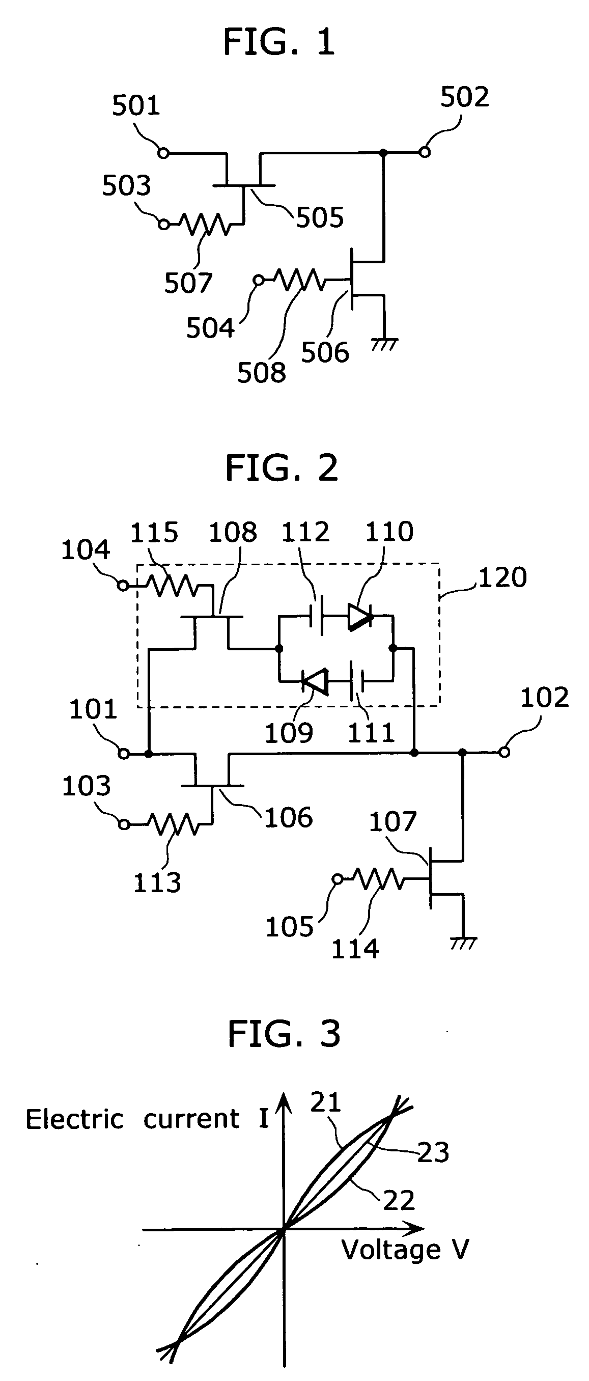
[0029]FIG. 2 is a circuit diagram showing a semiconductor switch according the first embodiment of the present invention.

[0030] Such semiconductor switch is made up of: an input terminal 101; an output terminal 102; a through FET 106 that is connected serially to the signal path between the input terminal 101 and the output terminal 102; a shunt FET 107 that is connected in between the output terminal 102 and the ground; and a distortion reducing circuit 120 that is connected in parallel with the through FET 106. Note that the through FET 106 forms a first semiconductor circuit and the distortion reducing circuit 120 forms a second semiconductor circuit.

[0031] The distortion reducing circuit 120, which is a circuit for approximating the current-voltage characteristics of the semiconductor switch to be linear, is made up of: a first diode 109 and a second diode 110 that are placed in parallel with each other; a first constant voltage source 111 and a second constant voltage source ...

second embodiment

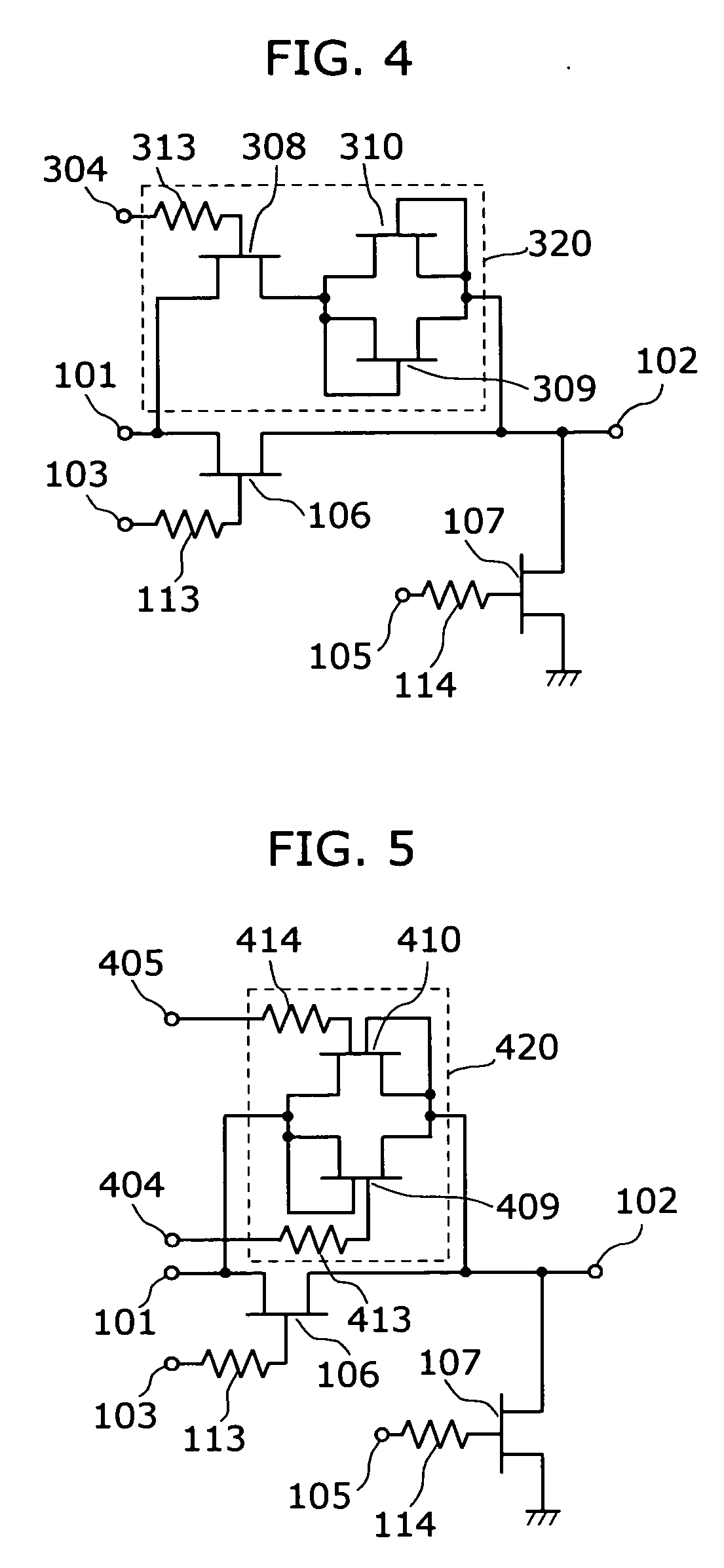
[0039]FIG. 4 is a circuit diagram showing a semiconductor switch according to the second embodiment of the present invention.

[0040] Such semiconductor switch is different from the semiconductor switch of the first embodiment in the structure of its distortion reducing circuit 320 that is connected in parallel with the through FET 106. The semiconductor switch of the second embodiment is made up of an input terminal 101, an output terminal 102, a through FET 106, a shunt FET 107, and a distortion reducing circuit 320 that is connected in parallel with the through FET 106. Note that the distortion reducing circuit 320 forms the second semiconductor circuit.

[0041] The distortion reducing circuit 320, which is a circuit for approximating the current-voltage characteristics of the semiconductor switch to be linear, is made up of: a first FET 309 and a second FET 310 that are connected in parallel with each other; and a FET 308 that is connected serially to the first FET 309 and the sec...

third embodiment

[0045]FIG. 5 is a circuit diagram showing a semiconductor switch according to the third embodiment of the present invention.

[0046] Such semiconductor switch is different from the semiconductor switch of the second embodiment in the structure of its distortion reducing circuit 420 that is connected in parallel with a through FET 106. The semiconductor switch of the third embodiment is made up of an input terminal 101, an output terminal 102, a through FET 106, a shunt FET 107, and a distortion reducing circuit 420 that is connected in parallel with the through FET 106. Note that the distortion reducing circuit 420 forms the second semiconductor circuit.

[0047] The distortion reducing circuit 420, which is a circuit for approximating the current-voltage characteristics of the semiconductor switch to be linear, is made up of a first dual gate FET 409 and a second dual gate FET 410 that are connected in parallel with each other. In this structure, one of the gates and the source or the...


PUM


Abstract

The present invention, which aims at providing a semiconductor switch capable of reducing harmonic distortion, is made up of: an input terminal 101; an output terminal 102; a through FET 106 that is connected serially to the signal path between the input terminal 101 and the output terminal 102; a shunt FET 107 that is connected in between the output terminal 102 and the ground; and a distortion reducing circuit 120 that is connected in parallel with the through FET 106. In this semiconductor switch, the distortion reducing circuit 120 includes: a first diode 109 and a second diode 110 that are placed in parallel with each other; a first constant voltage source 111 and a second constant voltage source 112 that are placed in parallel with each other; and a FET 108.

Description

BACKGROUND OF THE INVENTION [0001] (1) Field of the Invention [0002] The present invention relates to a semiconductor switch for use with a mobile communication device, and particularly to a high-frequency semiconductor switch that is used for switching between signal transmission and reception in an antenna of a mobile phone or the like. [0003] (2) Description of the Related Art [0004] With the recent developments in the field of mobile communications, a small, low-power high-frequency semiconductor switch has been desired as a semiconductor switch dedicated to switching between signal transmission and reception in an antenna of a mobile phone or the like. In these days, a semiconductor switch that utilizes a gallium arsenide field-effect transistor that is superior in terms of power consumption is used instead of the mainstream semiconductor switch that utilizes a silicon PIN diode. [0005] The following describes a high-frequency semiconductor switch that utilizes such a field-eff...

Claims


Application Information

Patent Timeline
IPC IPC(8): H01P1/15H03K17/06H03K17/687H04B1/44
CPCH03K17/6871H03K17/063
Inventor HIKITA, MASAHIROYANAGIHARA, MANABUUEDA, DAISUKE
Owner PANASONIC CORP
Why Eureka
Try Eureka