Semiconductor device with flowable insulation layer formed on capacitor and method for fabricating the same

a flowable, capacitor technology, applied in semiconductor devices, semiconductor/solid-state device details, capacitors, etc., can solve the problems of generating plasma damage on the bottom layer consisting of capacitors, and the inability to perform a low-temperature process with bpsg, etc., to achieve good planarization characteristics

Active Publication Date: 2005-12-01
SK HYNIX INC
View PDF17 Cites 131 Cited by
  • Summary
  • Abstract
  • Description
  • Claims
  • Application Information

AI Technical Summary

Benefits of technology

[0015] It is, therefore, an object of the present invention to provide a semiconductor device with a flowable insulation layer formed on a capacitor by performing a low-temperat

Problems solved by technology

Especially in this drawing, a problem related to the conventional method for forming the insulation layer on the capacitor is depicted.
Meanwhile, to remove the cavity 20 of the insulation layer D, a high density plasma-chemical vapor deposition (HDP-CVD) method having excellent planarization and step-coverage characteristics can be used to form the insulation layer D. However, the deposition mechanism of the HDP-CVD method is a repeating steps of etching and d

Method used


Image

  • Semiconductor device with flowable insulation layer formed on capacitor and method for fabricating the same
  • Semiconductor device with flowable insulation layer formed on capacitor and method for fabricating the same
  • Semiconductor device with flowable insulation layer formed on capacitor and method for fabricating the same

Examples


first embodiment

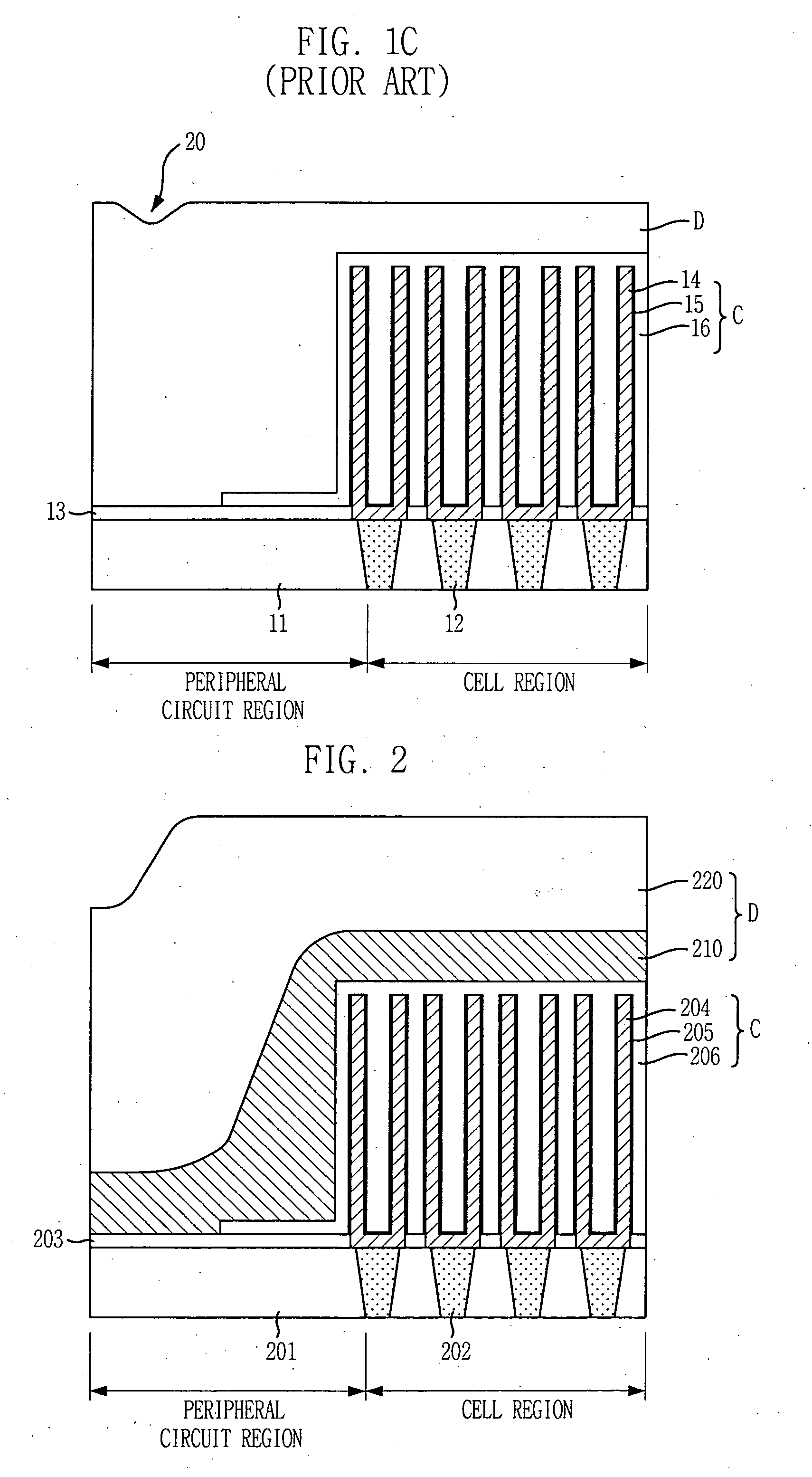
[0026] First, FIG. 2 shows one exemplary substrate structure in accordance with the present invention.

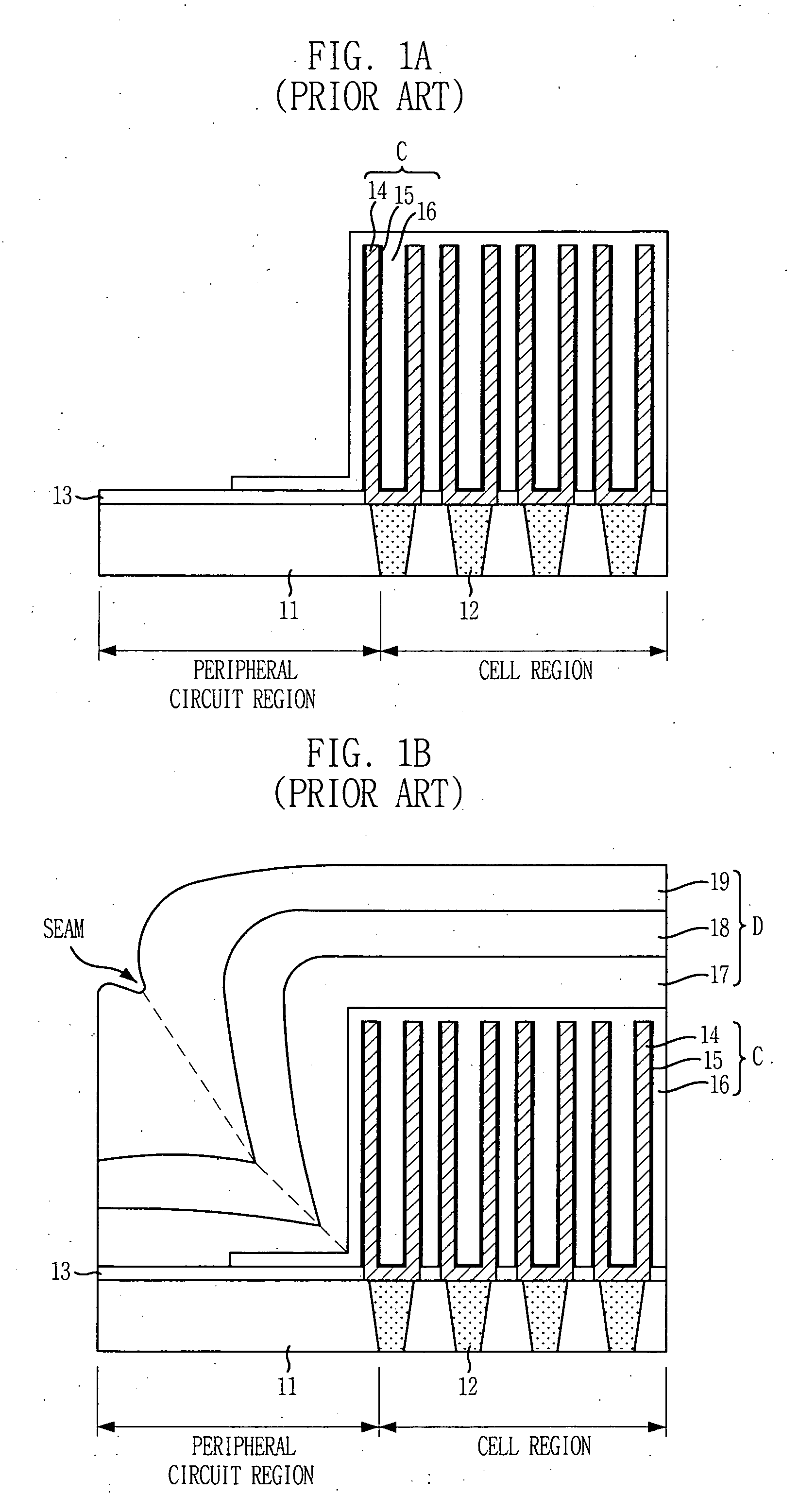
[0027] As shown, a plurality of capacitors C are formed on a substrate provided with a first insulation layer 201, contact plugs 202 and an etch stop layer 203. Each of the capacitors C includes a lower electrode 204 being contacted to the contact plug 202 and having a cylinder shape, a dielectric layer 205 covering the lower electrode 204 and an upper electrode 206 formed on the dielectric layer 205. The capacitors C are formed in a typical DRAM cell region and are not formed in a peripheral region. Hence, there exists a height difference of at least approximately 10,000 Å in a boundary between the cell region and the peripheral region.

[0028] Subsequently, a flowable insulation layer 210 that does not generate a seam in region where a height difference is high by having flowability during the deposition of the flowable insulation layer 210 is formed on the capacitor C.

[0029] Espe...

second embodiment

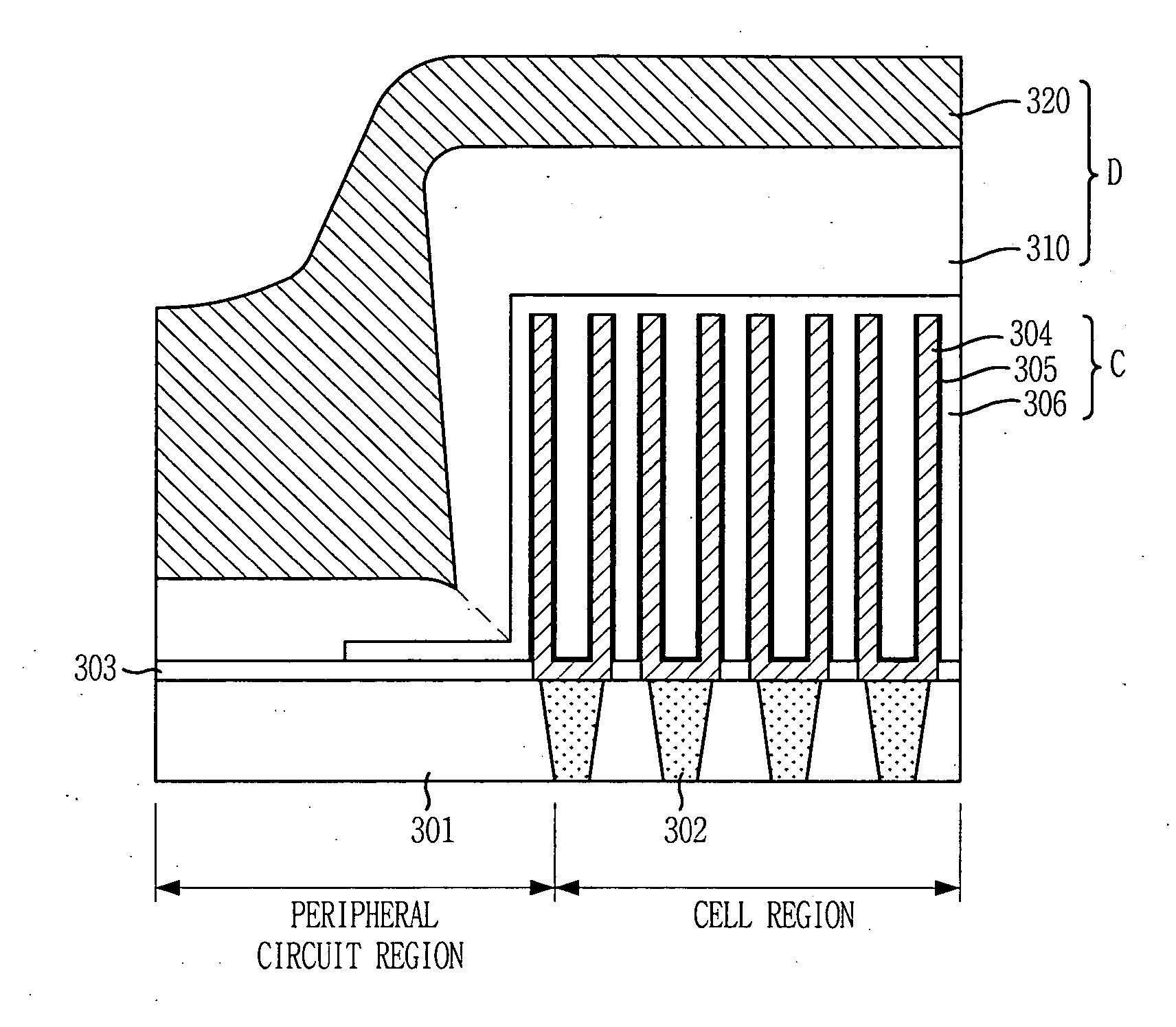
[0036]FIG. 3 is a cross-sectional view showing another exemplary substrate structure, wherein an insulation layer is formed on a capacitor in accordance with the present invention.

[0037] Referring to FIG. 3, a plurality of capacitors C are formed on a substrate provided with a first insulation layer 301, contact plugs 302 and an etch stop layer 303. Each of the capacitors C includes a lower electrode 304 being contacted to the corresponding contact plug 302 and having a cylinder shape, a dielectric layer 305 covering the lower electrode 304 and an upper electrode 306 formed on the dielectric layer 305. The capacitor C is formed in a typical DRAM cell region and is not formed on a peripheral region, thereby exhibiting a height difference of at least 10,000 Å in a boundary between the cell region and the peripheral region.

[0038] Subsequently, the USG-based insulation layer 310 formed by a PECVD method is formed on the capacitors C. At this time, a deposited thickness of the USG-based...

third embodiment

[0043]FIG. 4 is a cross-sectional view of a substrate structure, wherein an insulation layer is formed on a capacitor in accordance with the present invention.

[0044] Referring to FIG. 4, a plurality of capacitors C are formed on a substrate provided with a first insulation layer 401, contact plugs 402 and an etch stop layer 403. Each of the capacitors C includes a lower electrode 404 being contacted to the corresponding contact plug 402 and having a cylinder shape, a dielectric layer 405 covering the lower electrode 404 and an upper electrode 406 formed on the dielectric layer 405. The capacitor C is formed in a typical DRAM cell region and is not formed in a peripheral region, thereby exhibiting a height difference of at least 10,000 Å in a boundary between the cell region and the peripheral region.

[0045] Subsequently, USG-based insulation layer 410 is formed on the substrate provided with the plurality of capacitors C with use of a PECVD method. At this time, the USG-based insula...


PUM


Abstract

Disclosed is a semiconductor device with a flowable insulation layer formed on a capacitor and a method for fabricating the same. Particularly, the semiconductor device includes: a capacitor formed on a predetermined portion of a substrate; an insulation layer formed by stacking a flowable insulation layer and an undoped silicate glass layer on a resulting substrate structure including the substrate and the capacitor; and a metal interconnection line formed on the insulation layer. The method includes the steps of: forming a capacitor on a predetermined portion of a substrate; forming an insulation layer by stacking a flowable insulation layer and an undoped silicate glass layer on a resulting substrate structure including the substrate and the capacitor; and forming a metal interconnection line on the insulation layer.

Description

FIELD OF THE INVENTION [0001] The present invention relates to a semiconductor device; and more particularly, to a semiconductor device with an insulation layer on a capacitor and a method for fabricating the same. DESCRIPTION OF RELATED ARTS [0002] As is known well, a trend in micronization and large scale of integration of a semiconductor memory device is highly demanded to secure enough capacitance of a capacitor included in a dynamic random access memory (DRAM) cell. In order to obtain enough capacitance, a dielectric material is formed by stacking aluminum oxide (Al2O3) and hafnium oxide (HfO2), or an upper electrode and a lower electrode of a capacitor are formed by using a metal such as titanium nitride (TiN). [0003] Accordingly, in case of forming an insulation layer on top of the capacitor, the insulation layer should be formed essentially through a low-temperature process to prevent degradation of bottom layers of the capacitor for instance oxidization of a metal, degradat...

Claims


Application Information

Patent Timeline
IPC IPC(8): H01L21/02H01L27/108H01L21/8242H01L23/532
CPCH01L21/02134H01L21/02137H01L21/02164H01L21/022H01L21/02211H01L21/02271H01L28/91H01L21/02282H01L21/3124H01L21/31633H01L23/53295H01L27/10814H01L27/10894H01L21/02274H01L2924/0002H10B12/315H10B12/09H01L2924/00H10B12/00
Inventor AHN, SANG-TAESHEEN, DONG-SUNSONG, SEOK-PYOSHIN, JONG-HAN
Owner SK HYNIX INC
Why Eureka
Try Eureka