

Charged particle beam exposure system
a charge particle and beam technology, applied in the field of charge particle beam exposure systems, can solve the problems of correction values, homogeneity of beamlets, limited system output, etc., and achieve the effect of improving the performance of known charge particle beam exposure apparatus
- Summary
- Abstract
- Description
- Claims
- Application Information
AI Technical Summary
Benefits of technology
Problems solved by technology
Method used
Image

Examples
Embodiment Construction
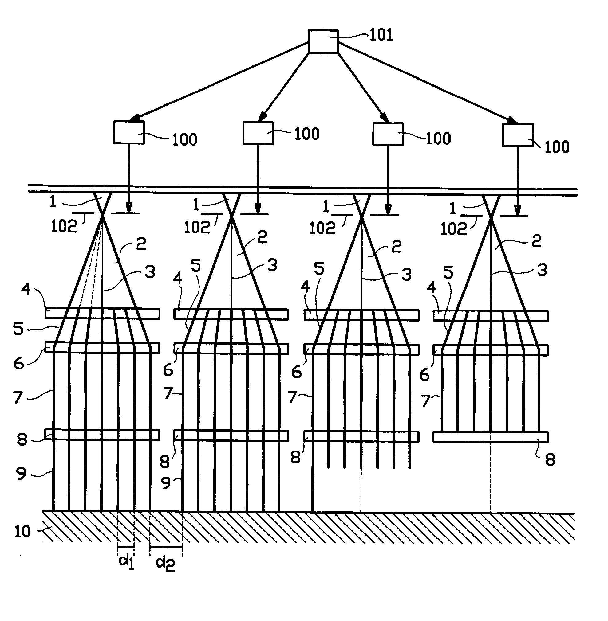
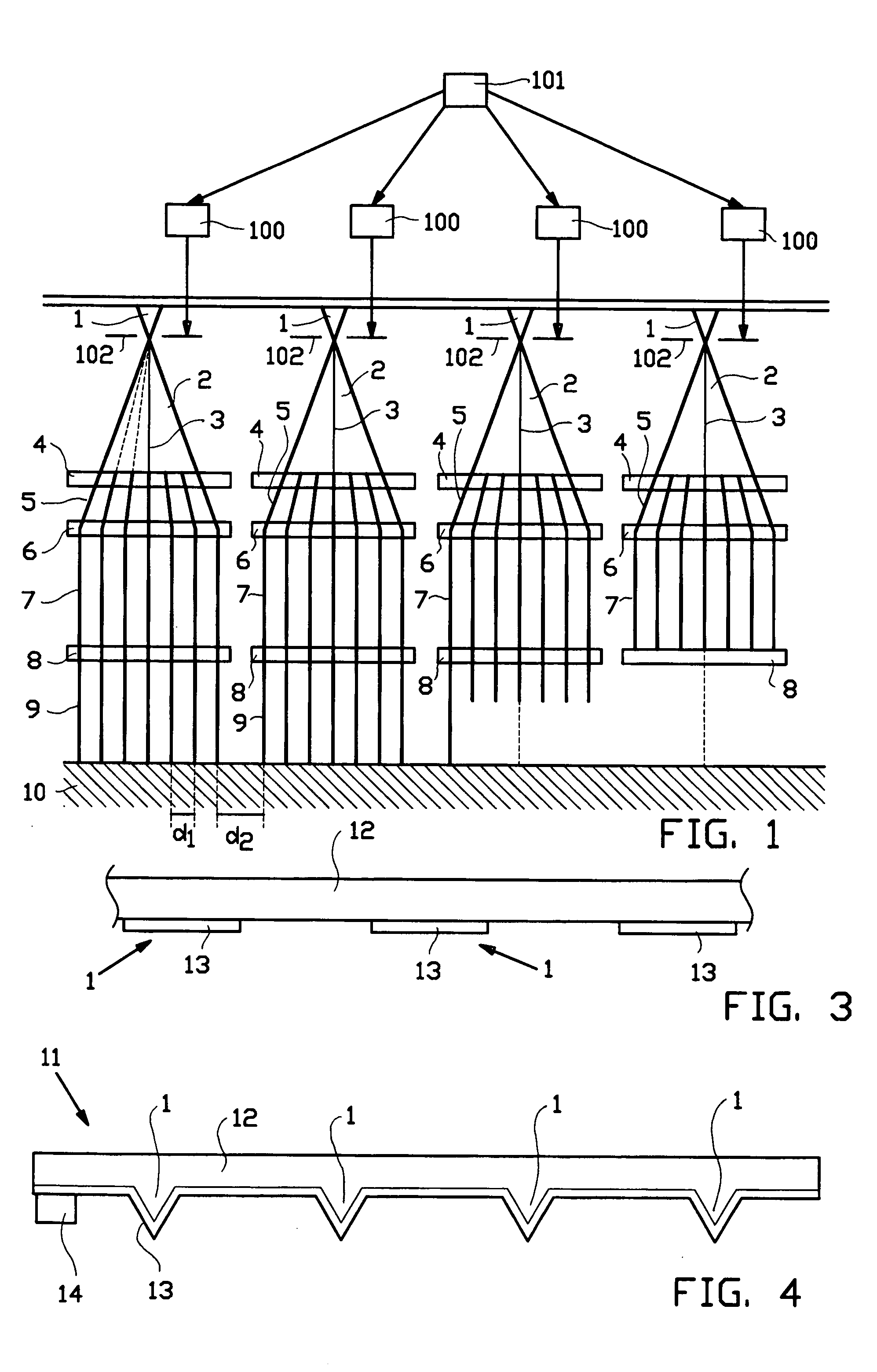
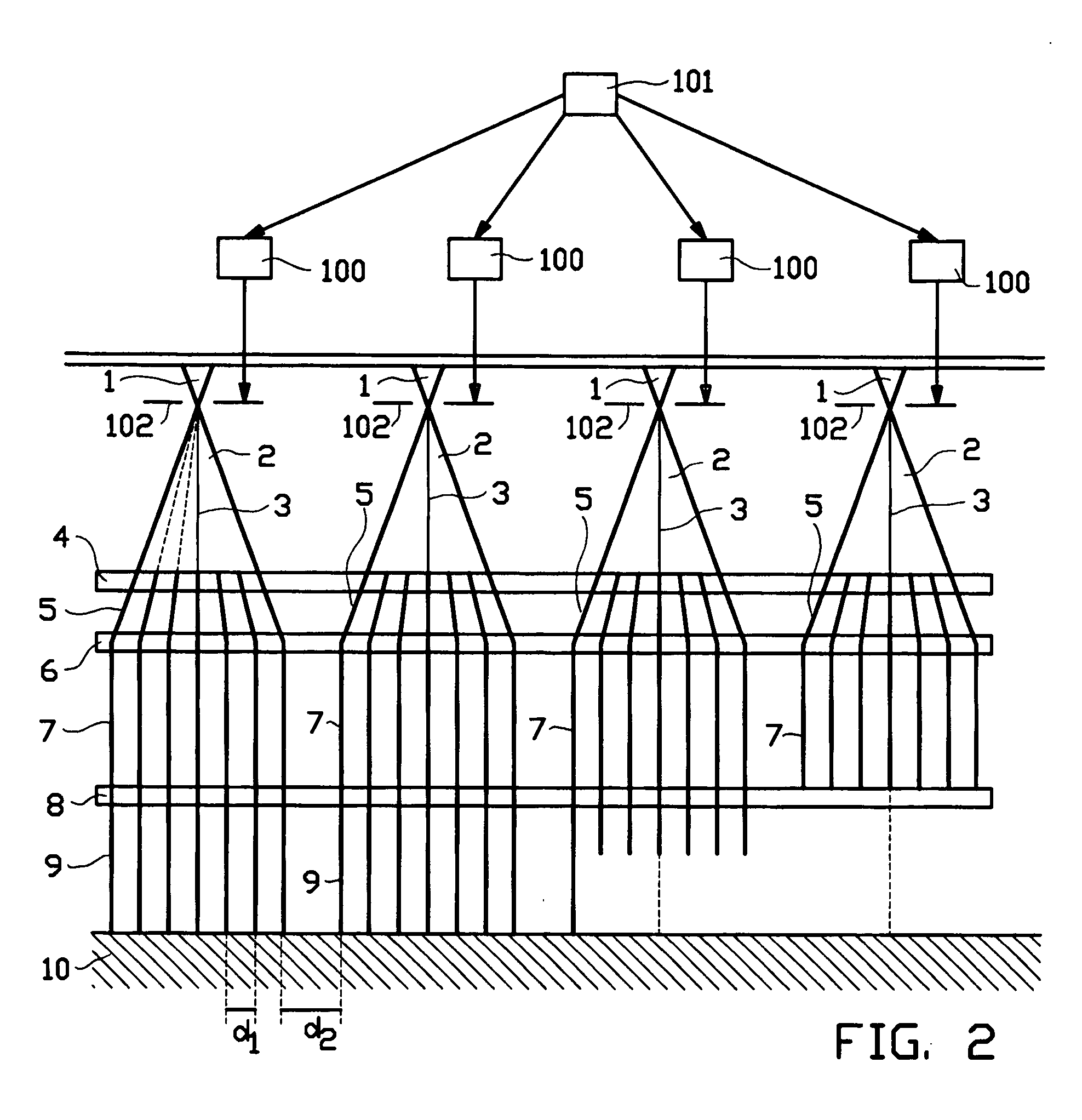
[0038] An embodiment of the present invention is schematically shown in FIG. 1. Electrons are emitted from several electron sources 1. The beam generator of the device has sources 1, each source 1 emitting an electron beam.
[0039] An illumination system (4, 6, 8) focuses and collimates each of the emitted electron beams 2 to illuminate a desired area on an aperture plate or aperture plates 4 uniformly.
[0040] The illumination system can be combined with all the features described in applicants co-pending patent applications U.S. 60 / 453,745 of Mar. 10, 2003, U.S. Ser. No. 10 / 600,953 of Jun. 20, 2003, U.S. Ser. No. 10 / 692,632 of Oct. 24, 2003, U.S. 60 / 491,475 of Jul. 30, 2003, and U.S. 60 / 473,810 of May 28, 2003, U.S. Ser. No. 10 / 699,246 of Oct. 30, 2003, or family members or continuations of these U.S. patent applications, which are all incorporated by reference as if fully set forth. All the devices, combinations thereof and specific elements, in most cases described for single beam...
PUM
 Abstract
Description
Claims
Application Information