Electron-emitting device, electron source, picture display unit and manufacturing process therefor

a technology of electron emission and electron source, which is applied in the manufacture of electric discharge tubes/lamps, discharge tubes with screens, discharge tubes luminescnet screens, etc., can solve the problems of overdischarge remarkably deteriorating the electron emission characteristics of the device, unstable potential of the surface of the insulating substrate, and unstable trajectory of the projected electron beam, so as to reduce the strain on the driving integrated circuit, reduce the cost of the panel, and easy to form a high resistivity film

Inactive Publication Date: 2005-12-08
CANON KK
View PDF7 Cites 13 Cited by
  • Summary
  • Abstract
  • Description
  • Claims
  • Application Information

AI Technical Summary

Benefits of technology

[0011] Objects of the present invention are to prevent a malfunction of the above-mentioned electron-emitting device and an electron source and an image display apparatus having the electron-emitting device caused by electrostatic charge, by easily forming a high resistivity film for stabilizing electron emission characterist

Problems solved by technology

Such an electron source substrate has had the problem that the electric potential of the surface of an insulating substrate becomes unstable due to the emission of electrons from an electron-emitting device, and the trajectory of a projected electron beam becomes unstable.
In addition, when charged particles such as electrons and ions are injected into the surface of an insulating substrate, the substrate produces secondary electrons, but particularly under a high electric field, it causes overdischarge, and it is experimentally confirmed that the overdischarge remarkably deteriorates electron emission characteristics of a device and destroys the device in the worst case.
However, when a high resistivity film is formed on the whole surface of a substrate including electron-emitting devices, a leak current passes between device electrodes through the high resistivity film, and there are cases where the amperage is unexpectedly large.
When the high resistivity film is thickly formed and acquires low sheet resistance, such a film passes a leak current through the high resistivity film itself when the device is not driven and applied voltage is low, and has caused a p

Method used


Image

  • Electron-emitting device, electron source, picture display unit and manufacturing process therefor
  • Electron-emitting device, electron source, picture display unit and manufacturing process therefor
  • Electron-emitting device, electron source, picture display unit and manufacturing process therefor

Examples


embodiments

Embodiment 1

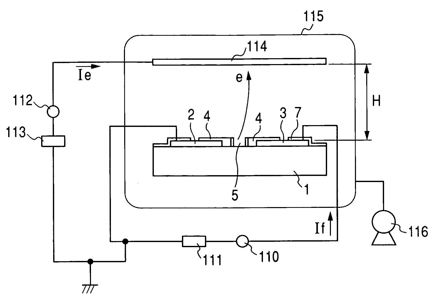
[0100] An electron source having a configuration shown in FIG. 10 was produced according to the steps shown in FIGS. 2A and 2B to 6A and 6B.

[0101] An electron source substrate 91 to be used was prepared by applying a SiO2 material on a glass plate of PD200 containing little alkaline component (a product made by Asahi glass Co.) with the thickness of 2.8 mm, and baking it into a SiO2 film with the thickness of 100 nm for a sodium blocking layer.

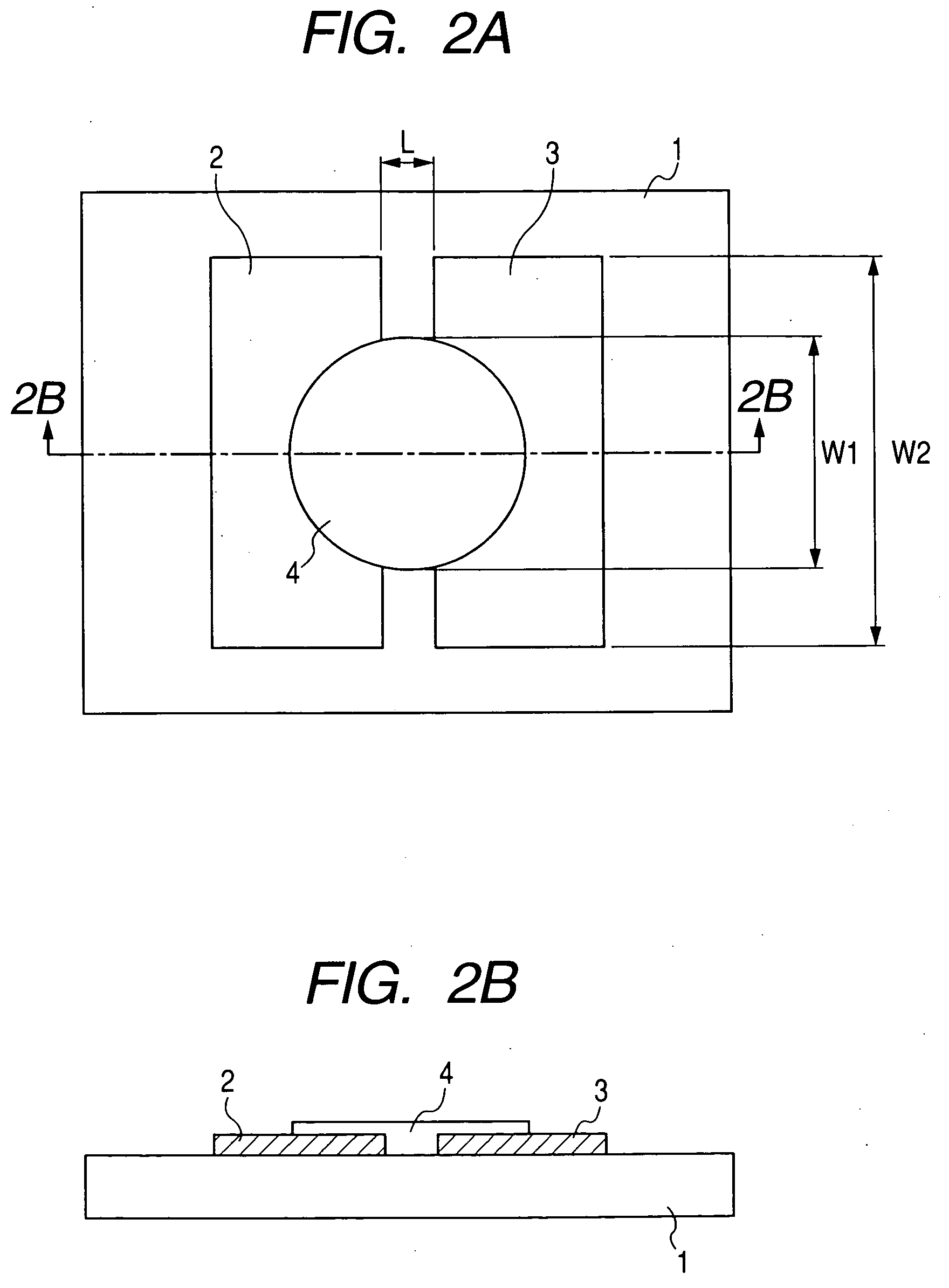
[0102] On the above described substrate 91, device electrodes 2 and 3 were formed by the steps of: sequentially forming the film of Ti with the thickness of 5 nm as an underlayer, and of Pt with the thickness of 40 nm thereon with a sputtering technique; subsequently applying a photo resist thereon; and patterning the film with a photolithographic process consisting of the serial steps of exposure, development and etching.

[0103] A column directional wiring 92 was formed by printing a linear pattern of an Ag paste (a product mad...

embodiment 2

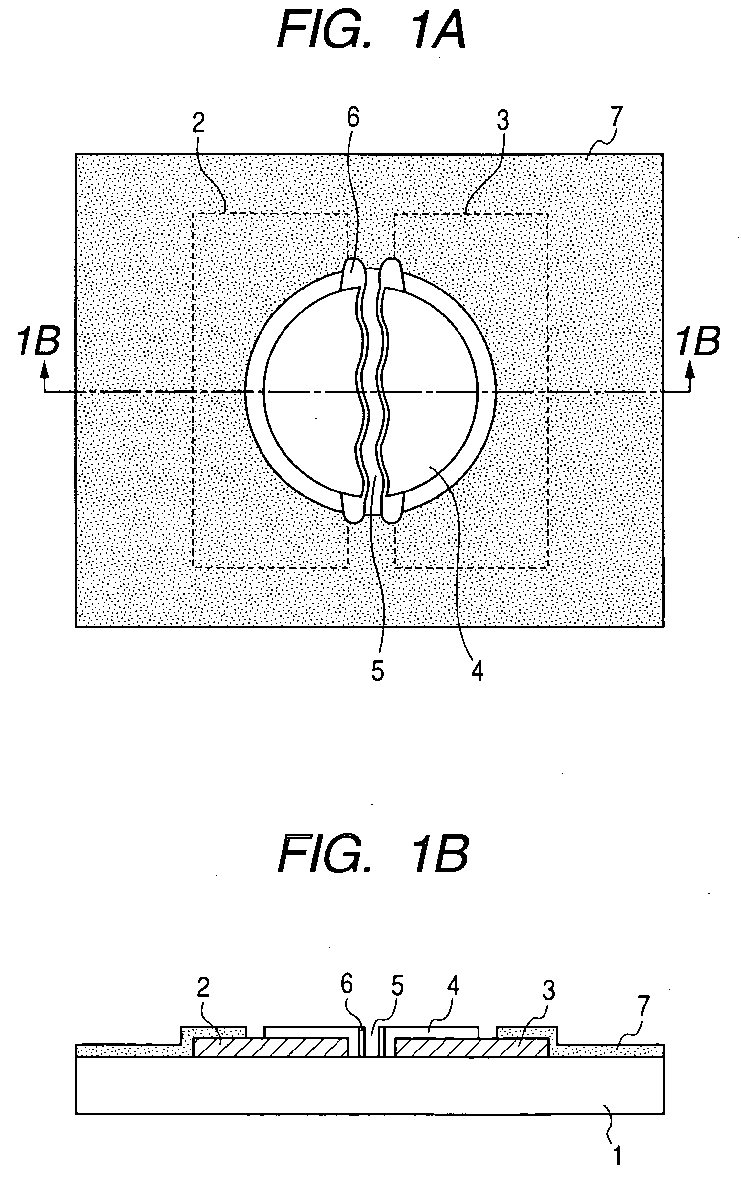
[0119] An electron source was produced with a similar process to that in the embodiment 1, except that in the present embodiment, the precursor 41 of a high resistivity film was precedently applied to the whole surface of a substrate 91 after an electroconductive thin film 4 was formed, and subsequently the material solution of a water-repellent film 31 was applied onto the electroconductive thin film 4 of each unit with an ink jet method to repel the precursor 41 of the high resistivity film on the electroconductive thin film 4.

[0120] In the obtained electron source, a carbon film 6 is formed so as to reach a high resistivity film 7 from the intersecting point of the edge of an electroconductive thin film 4 with a fissure 5, in each electron-emitting device, and the high resistivity film 7 and the carbon film 6 showed similar surface resistance to those in the embodiment 1. In addition, as a result of having evaluated the electron emission characteristics of the obtained electron ...


PUM


Abstract

An object of the present invention is to prevent a device portion from being electrostatically charged with the use of the high resistivity film, and at the same time prevent a leak current passing the device portion due to an existing high resistivity film, in an electron source with the use of a surface-conduction electron-emitting device. This process for manufacturing the electron-emitting device comprises the steps of: forming an electroconductive thin film 4 astride device electrodes; forming the high resistivity film 7 in a region except the electroconductive thin film 4 and a perimeter thereof; subjecting the electroconductive thin film 4 to forming processing, to form a fissure 5 therein; and depositing a carbon film 6 inside the fissure 5 and in a region reaching the high resistivity film 7 from the edge of the fissure 5, by applying voltage between device electrodes 2 and 3 under an atmosphere containing a carbon compound.

Description

BACKGROUND OF THE INVENTION [0001] 1. Field of the Invention [0002] The present invention relates to a surface-conduction electron-emitting device provided with an anti-static function, an electron source using it, further a picture display unit with the use of the electron source, and manufacturing processes for the same. [0003] 2. Related Background Art [0004] In recent years, a flat panel display using a surface-conduction electron-emitting device has been developed actively. The above described electron-emitting device has a pair of device electrodes placed at a predetermined space apart from each other on an insulating substrate normally made of a glass substrate, and an electroconductive thin film arranged astride the above described device electrodes, and a fissure formed inside the above described electroconductive thin film by energization processing for the above described electroconductive thin film; and emits electrons from the above described fissure through applying vo...

Claims


Application Information

Patent Timeline
IPC IPC(8): H01J1/316H01J1/62H01J9/02H01J31/12H01J63/04
CPCH01J1/316H01J2201/3165H01J31/127H01J9/027
Inventor TAKADA, KUNIO
Owner CANON KK
Why Eureka
Try Eureka