Semiconductor device and manufacturing method for same

a semiconductor and manufacturing method technology, applied in semiconductor devices, digital storage, instruments, etc., can solve the problems of inability to perform non-destructive read-out, unstable crystals, and difficulty in processing materials, etc., to achieve easy implementation of non-volatile memory, increase resistivity value, and low power consumption

Inactive Publication Date: 2005-12-08
SHARP KK
View PDF6 Cites 28 Cited by
  • Summary
  • Abstract
  • Description
  • Claims
  • Application Information

AI Technical Summary

Benefits of technology

[0019] Firstly, the manufacturing method for a semiconductor device is essentially characterized in that: a variable resistor film (PCMO film) is formed in the amorphous state or in the polycrystalline state above a semiconductor substrate in the film formation step and the PCMO film is thermally processed in an oxidizing atmosphere of a gas that is selected from types of gasses that structurally include nitrogen atoms in the thermal processing step, and thereby, ON radicals can be introduced into positions of oxygen deficiency defects in this PCMO film. N of ON that has been inserted into a position of oxygen deficiency defect has three ligands, and therefore, the three-dimensionally coupled network structure of the PCMO perovskite structure is locally broken down. This breakdown in the crystal structure works so as to increase the resistivity value, and consequently, it becomes possible to form a PCMO film having a desired resistivity value. As a result of this, it becomes possible to easily implement a non-volatile memory where nondestructive read-out and operation with low power consumption are made possible by applying the manufacturing method for a semiconductor device that is firstly characterized by the present invention to a non-volatile memory device having a PCMO film.
[0020] Secondly, the manufacturing method for a semiconductor device is essentially characterized in that: a variable resistor film (PCMO film) is formed in the amorphous state or in the polycrystalline state above a semiconductor substrate in the film formation step and the first thermal processing is carried out in a non-oxidizing atmosphere, and thereby, oxygen within this PCMO film is diffused to the outside so as to introduce oxygen deficiency defects in the first thermal processing step. Subsequently, the second thermal processing is carried out in an oxidizing atmosphere of a gas selected from types of gasses that structurally include ni...

Problems solved by technology

However, storage information is electrically stored in a memory device, and therefore, a specific information storing structure is required, making reduction in voltage and power consumption difficult.
Meanwhile, though FeRAMs are superior to flash memories, from the point of view of write-in speed, power supply voltage and power consumption, they have the disadvantage of not being able to perform nondestructive read-out.
The PCMO film in this amorphous condition is crystallized in a thermal process during the semiconductor manufacturing proce...

Method used


Image

  • Semiconductor device and manufacturing method for same
  • Semiconductor device and manufacturing method for same
  • Semiconductor device and manufacturing method for same

Examples


first embodiment

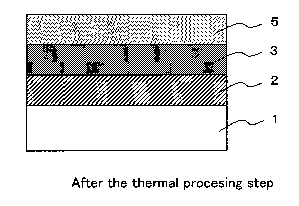
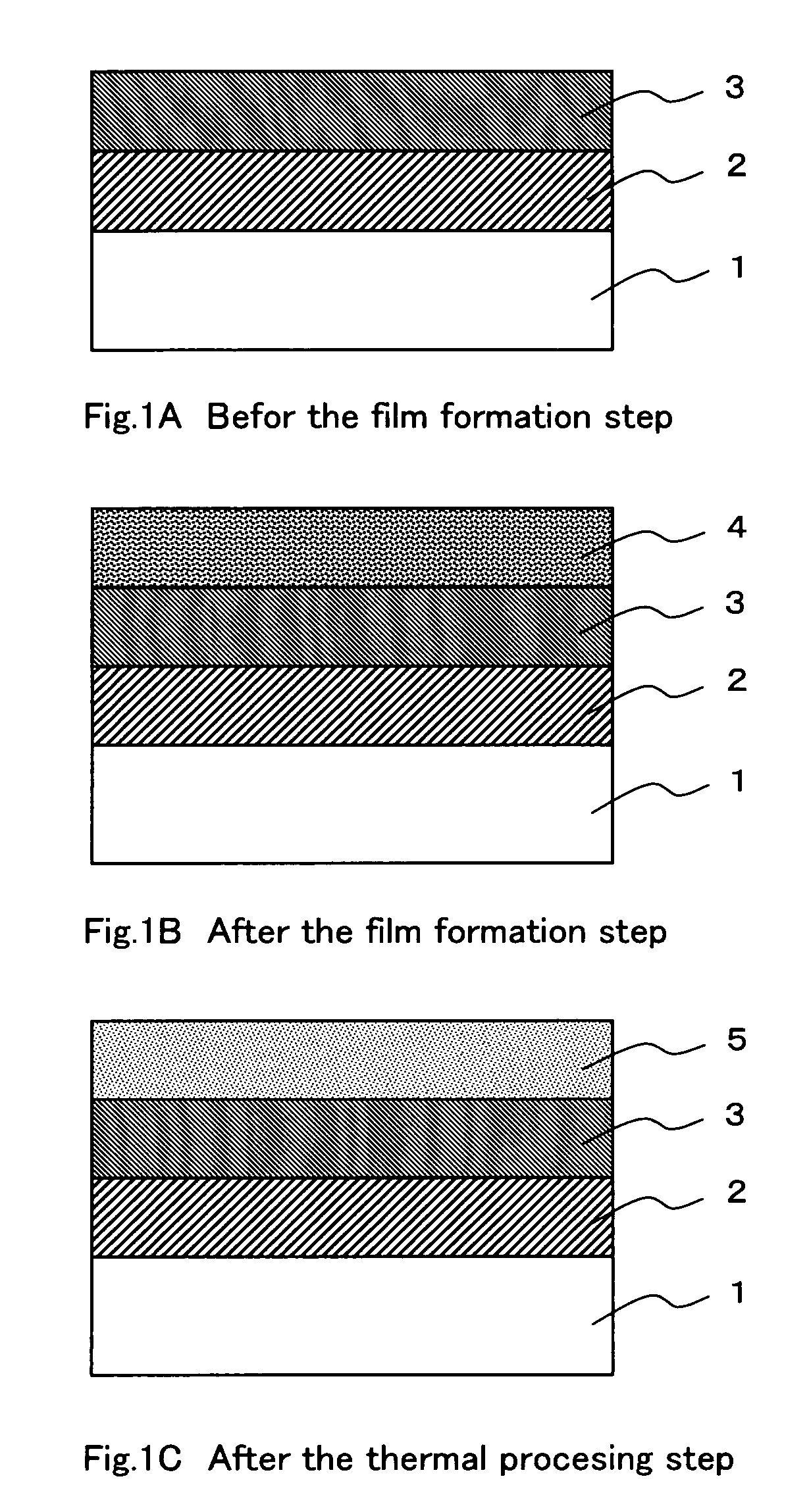
[0030] As shown in FIG. 1, first, an insulating film 2 and a high melt point metal film 3 are formed on the surface of a semiconductor substrate 1 according to a known technology. An Si substrate 1 having a thickness of 750 μm and a diameter of approximately 200 mm (8 inches), for example, is prepared as the semiconductor substrate 1, and 1 μm of a silicon oxide film 2 (insulating film 2) and 300 nm of a Pt film 3 (high melt point metal film 3) are deposited using a commercially available CVD unit (FIG. 1A).

[0031] Subsequently, in the film formation step, 200 nm of a Pr0.7Ca0.3MnO3 film 4 (PCMO film 4) is deposited at a film formation temperature of 300° C. according to a PVD method (FIG. 1B). Here, it is desirable for the film thickness of PCMO film 4 to be in a range from 100 nm to 600 nm. The PCMO film that has been formed at 300° C. is in crystal form in an amorphous state where coupling between the respective component atoms that form the perovskite structure is incomplete, an...

second embodiment

[0038] Next, a second embodiment of the method of the present invention is described in reference to FIG. 2.

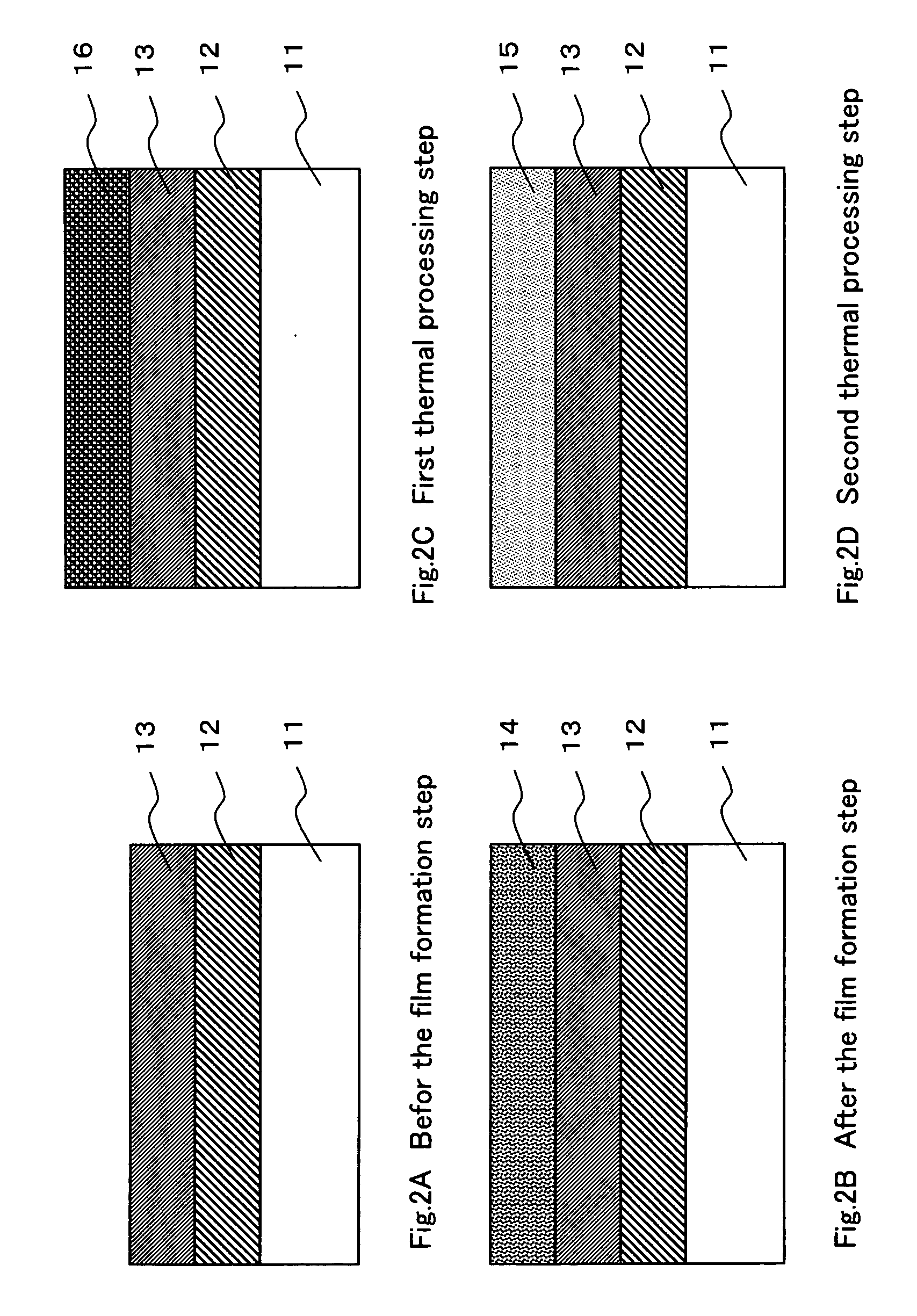
[0039] First, an insulating film 12 having a film thickness of 1 μm and a high melt point metal film 13 having a film thickness of 300 nm are sequentially deposited on a semiconductor substrate 11 (FIG. 2A). For example, a CVD-Si oxide film is used as the insulating film 12, and Pt is used as the high melt point metal film 13, respectively. The above described process is carried out in the same manner as in the first embodiment.

[0040] Subsequently, in the film formation step, 200 nm of a Pr0.7Ca0.3MnO3 film 14 (PCMO film 14) is deposited at a film formation temperature of 300° C. according to a PVD method (FIG. 2B). Here, it is desirable for the film thickness of the PCMO film 14 to be in a range from 100 nm to 600 nm, in the same manner as in the first embodiment.

[0041] Next, in the first thermal processing step, an annealing process is carried out on the semiconductor sub...

third embodiment

[0046] Next, the third embodiment of the method of the present invention is described in reference to FIG. 3.

[0047] First, an insulating film 22 having a film thickness of 1 μm and a high melt point metal film 23 having a film thickness of 300 nm are sequentially deposited on a semiconductor substrate 21 (FIG. 3A). For example, a CVD-Si oxide film is utilized as the insulating film 22, and Pt is utilized as the high melt point metal film 23, respectively.

[0048] Subsequently, in the film formation step, 200 nm of a Pr0.7Ca0.3MnO3 film 24 (PCMO film 24) is deposited at a film formation temperature of 300° C. according to a PVD method (FIG. 3B). Here, it is desirable for the film thickness of the PCMO film 24 to be a film thickness in a range from 100 nm to 600 nm, in the same manner as in the first and second embodiments.

[0049] Next, in the surface processing step, the semiconductor substrate 21 on which the PCMO film 24 has been deposited is exposed to a plasma atmosphere using a ...


PUM


Abstract

The thermal processing step of thermally processing a variable resistor film in an oxidizing atmosphere is carried out after the film formation step of forming a variable resistor film (PCMO film), and ON radicals are introduced into positions of oxygen deficiency defects in the PCMO film, and thereby, the three-dimensionally coupled network structure having the PCMO perovskite structure is locally broken down so as to increase the resistivity value.

Description

CROSS REFERENCE TO RELATED APPLICATTION [0001] This Nonprovisional application claims priority under 35 U.S.C. §119(a) on Patent Application No. 2004-169903 filed in Japan on Jun. 8, 2004, the entire contents of which are hereby incorporated by reference. BACKGROUND OF THE INVENTION [0002] 1. Field of the Invention [0003] The present invention relates to a semiconductor device that is provided with a variable resistor film made of a PrxCa1-xMnO3 film of which the electrical resistance changes through the application of electrical stress, as well as to a manufacturing method for the same. [0004] 2. Description of the Related Art [0005] Reduction in voltage and power consumption, as well as increase in speed, has been required in semiconductor devices, in particular, in CMOS devices, together with a requirement for energy conservation. The driving performance of MOS transistors that form CMOS devices have so far been secured as a result of miniaturization in the transistor structure, ...

Claims


Application Information

Patent Timeline
IPC IPC(8): H01L27/04H01L45/00H01L21/822H01L27/10G11C11/22
CPCH01L45/1625H01L45/1641H01L45/04H01L45/1233H01L45/147G11C13/0007G11C2213/31G11C13/0069H10N70/20H10N70/8836H10N70/041H10N70/026H10N70/826
Inventor NAKANO, TAKASHI
Owner SHARP KK
Why Eureka
Try Eureka