Receiving device and analog-to-digital conversion device

a technology of analog-to-digital conversion and receiving device, which is applied in the direction of pulse manipulation, line-transmission details, pulse technique, etc., can solve the problems of increasing the degree of difficulty in design, bringing about increased cost, and difficulty in downsizing circuits and simplifying processing, so as to facilitate delay design in view of timing, reduce power consumption, and increase circuit size

Inactive Publication Date: 2005-12-08
RENESAS ELECTRONICS CORP
View PDF8 Cites 14 Cited by
  • Summary
  • Abstract
  • Description
  • Claims
  • Application Information

AI Technical Summary

Benefits of technology

[0066] According to the present invention, by using the adaptive filter for executing adaptive equalization also as the filter of the type of which the coefficients can be changed for AD converter correction, sampling phase compensation of the AD converter can be achieved while r

Problems solved by technology

As described above, when the receiver is configured so that the correction circuit is provided, it is necessary to add a circuit, the processing, and the sequence unnecessary for a normal adaptive equalizer in the receiver, thus making it difficult to downsize the circuit and simplify the processing.
However, when a configuration is ma

Method used


Image

  • Receiving device and analog-to-digital conversion device
  • Receiving device and analog-to-digital conversion device
  • Receiving device and analog-to-digital conversion device

Examples


first embodiment

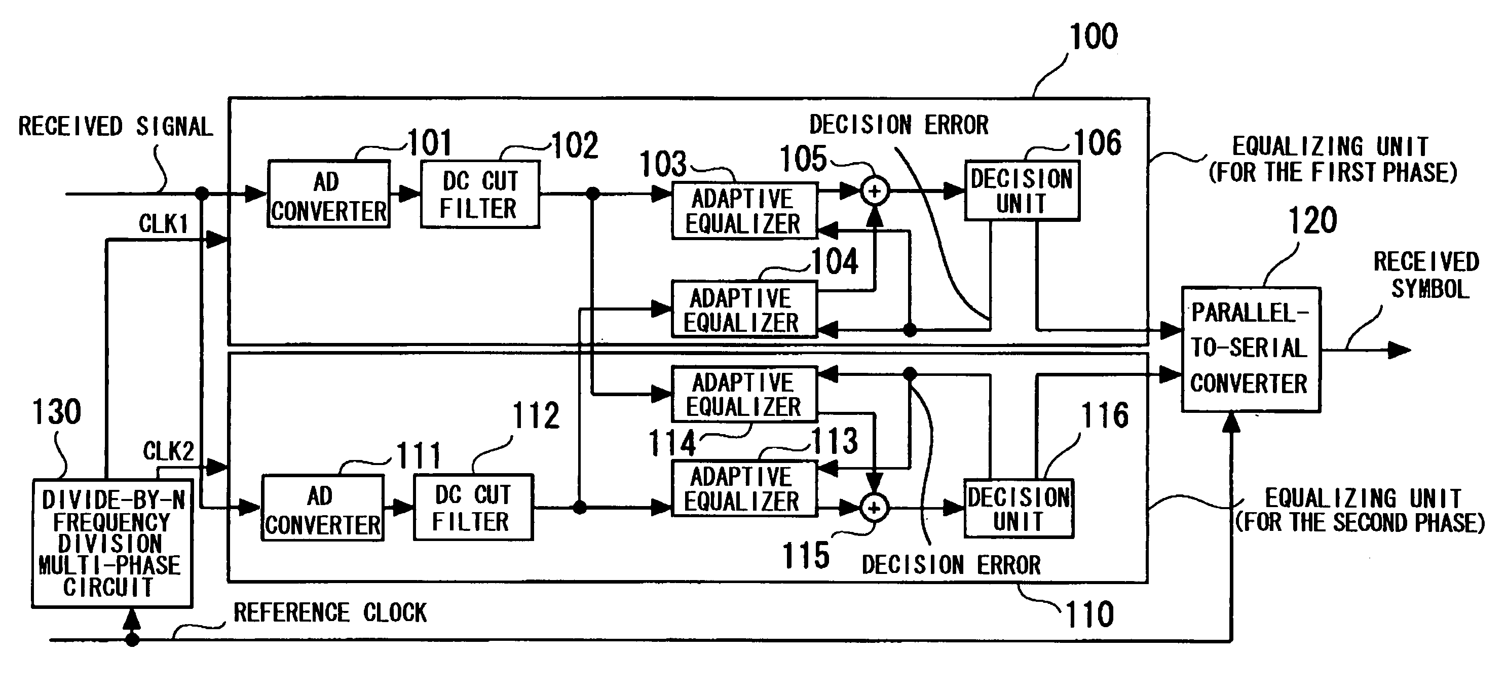
[0086]FIG. 1 is a diagram showing a configuration of a receiver according to the present invention. The receiver given below is employed as a receiver shown in FIGS. 2 and 3, for example.

[0087] Referring to FIG. 1, the receiver in the present embodiment includes the two AD converters 101 and 111, DC (direct-current) cut filters 102 and 112, the adaptive equalizers 103 and 104, the adaptive equalizers 113 and 114, adders 105 and 115, the decision units 106 and 116, a parallel-to-serial converter 120, and the divide-by-N frequency division multi-phase circuit 130. The AD converters 101 and 111 receive a received analog signal input and convert the analog signal to digital signals in response to the sampling clocks CLK1 and CLK2 of mutually different phases, for output. The DC cut filters 102 and 112 input the digital signals output from the two AD converters 101 and 111, respectively. The adaptive equalizers 103 and 104 input the outputs of the DC cut filters 102 and 112, respectively...

second embodiment

[0117] Referring to FIG. 7, the present embodiment employs the decision feedback equalizer 141 as in the second embodiment shown in FIG. 6, and further includes echo canceling units 150 and 160.

[0118] A serial-to-parallel converter 170 driven by the reference clock serially inputs even-numbered and odd-numbered transmission symbols one by one from a transmitter not shown, for conversion to parallel data. The serial-to-parallel converter 170 supplies a common transmission symbol (an even-numbered symbol) to adaptive equalizers (adaptive filters) 151 and 152, and supplies a common transmission symbol (an odd-numbered symbol) to adaptive equalizers (adaptive filters) 161 and 162.

[0119] The outputs of the adaptive equalizers 151 and 152 both driven by the sampling clock signal CLK2 supplied to an equalizing unit 110B are added by an adder 153, and the result of addition is supplied to one input to an adder 107 of the equalizing unit 100B. The outputs of the adaptive equalizers 161 and ...

fourth embodiment

[0123] Next, the present invention will be described. FIG. 8 is a diagram showing a specific example to which the present invention has been applied, and is the diagram showing a configuration of a receiver having an MIMO (Multiple-Input Multiple-Output) filter configuration. Referring to FIG. 8, the DC cut filters are omitted.

[0124] Referring to FIG. 8, a transmitter (TX) 401 transmits a symbol to a line 402 at a frequency fs. A time-interleaved AD conversion device (TI-ADC) 400 in a receiver is constituted from two AD converters connected in parallel, for sampling even-numbered data and odd-numbered data, respectively, in response to the sampling clock signal of mutually different phases and a frequency of fs / 2 obtained by dividing the fs by two. Each of the two AD converters includes a sampler 403 / 406, an adder 404 / 407 for adding the output of the sampler 403 / 406 to a DC offset (Offset 1 / Offset 2), and an amplifier 405 / 408 for inputting the output of the adder 404 / 407. The offset...


PUM


Abstract

Disclosed is a receiving device which comprises first and second AD converters for inputting a received analog signal and converting the analog signal to digital signals in response to sampling clock signals of mutually different phases, first and second adaptive equalizers for respectively receiving outputs of the first and second AD converters, third and fourth adaptive equalizers for respectively receiving outputs of the second and first AD converters, a first adder for adding the outputs of the first and second adaptive converters, a second adder for adding the outputs of the third and fourth adaptive equalizers, a first decision unit for receiving the output of the first adder, deciding a received symbol for output, and outputting a decision error, a second decision unit for receiving the output of the second adder, deciding a received symbol for output, and outputting a decision error, and a multiplexing circuit for multiplexing the received symbols output from the first and second decision units, for output. The decision error from the first decision unit is supplied to the first and second adaptive equalizers, and the decision error from the second decision unit is supplied to the third and fourth adaptive equalizers.

Description

FIELD OF THE INVENTION [0001] The present invention relates to a receiving device having an analog-to-digital conversion device. More specifically, the invention relates to a time-interleaved analog-to-digital conversion device and the receiving device having the analog-to-digital conversion device. BACKGROUND OF THE INVENTION [0002] Some examples of typical data transmission systems will be outlined in the below. First, an optical transmission system will be described with reference to FIG. 2. As shown in FIG. 2, in the transmission system using an optical fiber, in transmitters 10 and 19 on transmitting sides, transmission symbols (digital signals), each of which is the information transmission unit, are converted to analog signals by digital-to-analog converters not shown, and the analog signals are supplied to electric-to-optical converters 12 and 17 such as semiconductor lasers (LDs) and are output into optical fibers 14 and 15 from the electric-to-optical converters 12 and 17 ...

Claims


Application Information

Patent Timeline
IPC IPC(8): H03M1/12H04B3/06H03H21/00H03H7/30H03M1/10
CPCH03H21/0012H04L25/03038H04L25/03057H04L25/061H04L2025/0349H04L2025/03503H04L2025/03611
Inventor SHIDA, YASUNARI
Owner RENESAS ELECTRONICS CORP
Why Eureka
Try Eureka