Method of manufacturing nonvolatile semiconductor memory device

a non-volatile, memory device technology, applied in the direction of semiconductor devices, electrical devices, transistors, etc., can solve the problems of insufficient suppression of the leak current between the control gate electrode b>205/b> and the flowing gate electrode b>203/b>, and insufficient improvement of charge trapping properties, etc., to achieve excellent programming/erase endurance and charge trapping properties.

Active Publication Date: 2005-12-08
RENESAS ELECTRONICS CORP
View PDF7 Cites 37 Cited by
  • Summary
  • Abstract
  • Description
  • Claims
  • Application Information

AI Technical Summary

Benefits of technology

[0017] Interface state density (Dit) increases with programming / erase operation times when the oxidation conditions of ISSG are severe in an MONOS type nonvolatile memory, so that the ON current Id cannot be taken at the same memory gate voltage, thereby restricting the number of programming / erase operation. Moreover, there is a problem in that a large number of electron trap sites are produced in the oxide film; the sites deteriorate charge trapping properties.
[0019] An object of the present invention is to improve the attributes of a nonvolatile memory of a structure having a silicon oxide film on top of a silicon nitride film. In particular, the invention is directed to the improvement of programming / erase endurance and the prevention of deterioration of charge trapping properties without degrading the interfacial properties of a gate insulating film prior to formation of the silicon nitride film.
[0020] The most important feature of the present invention is to oxidize a silicon nitride film in an oxidizing atmosphere without hydrogen and to fabricate a silicon oxide film of 4 nm or more on top of the silicon nitride film. This is for the purpose of decreasing the interface state density of the gate oxide film formed prior to the silicon nitride film and suppressing the generation of electron trap sites in the oxide film. Specifically, the silicon oxide film is fabricated by an oxidation method using ozone of a high concentration. The silicon oxide film is formed under the process conditions satisfying L / U <2×10⁻³ [s], for instance, where the distance 803 between the ozone inlet and the wafer is set to L [m], and the ozone gas flow rate 802 is set to U [m / s]. Furthermore, with satisfying these conditions, a silicon oxide film of 4 nm or more is desirably formed under conditions of an ozone concentration of 20% or more and an ozone partial pressure of from 133 Pa to 20 kPa.
[0021] Use of the present invention enables the suppression of increases in the interface state density and the electron trap density of a transistor, thus greatly improving the reliability of the nonvolatile memory. In particular, the programming / erase endurance and charge trapping properties are improved.
[0023] With the combination of the above effects, the present invention can yield a nonvolatile memory excellent in programming / erase endurance and charge trapping properties.

Problems solved by technology

This poses the problem of an insufficient improvement in charge trapping properties.
Because of the same reason also, there is a problem in that the suppression of the leak current of the interlayer between the control gate electrode 205 and the flowing gate electrode 203 is insufficient even in the floating gate type nonvolatile memory.
Due to the above reasons, the above problems are presented.

Method used


Image

  • Method of manufacturing nonvolatile semiconductor memory device
  • Method of manufacturing nonvolatile semiconductor memory device
  • Method of manufacturing nonvolatile semiconductor memory device

Examples


embodiment 1

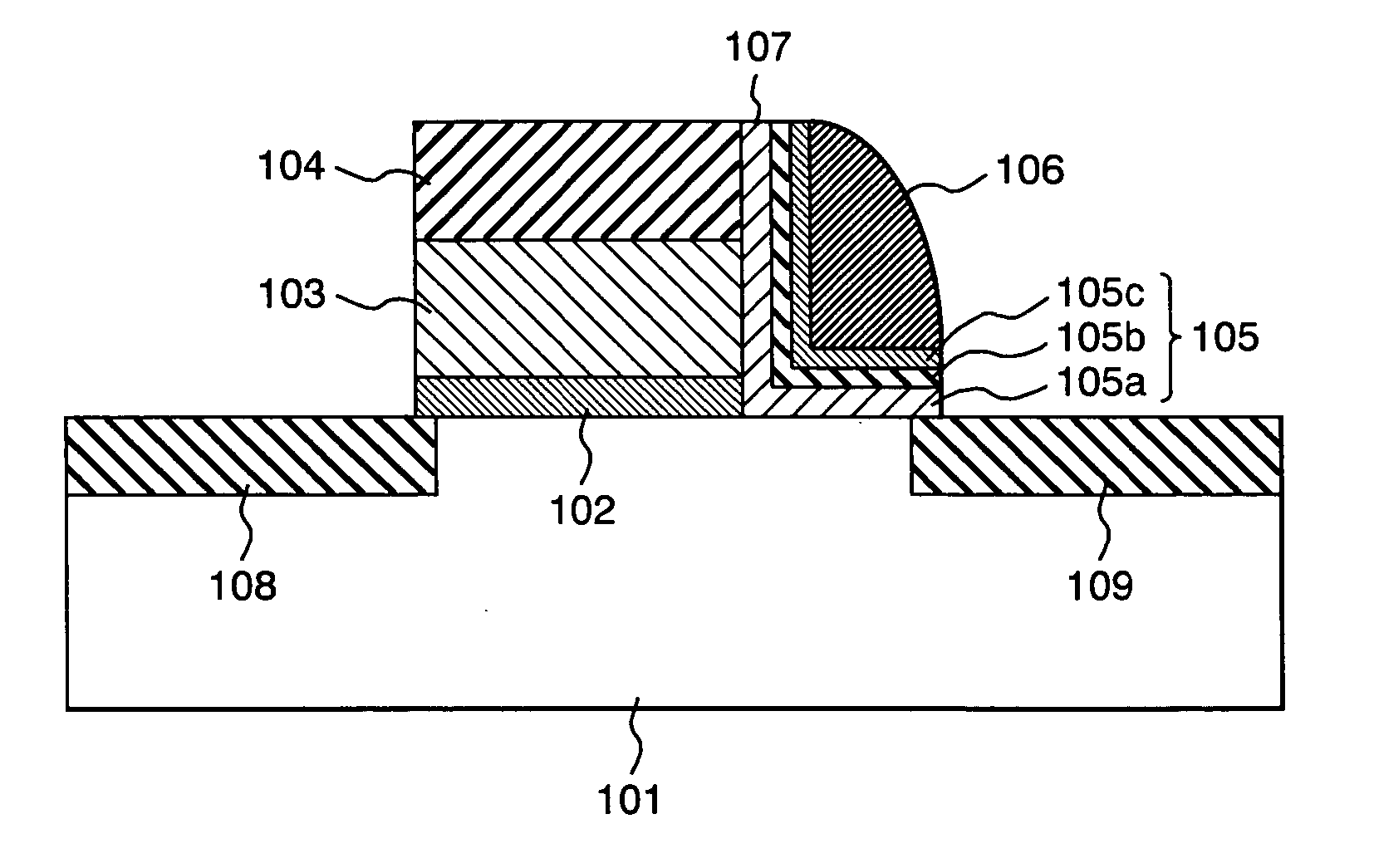
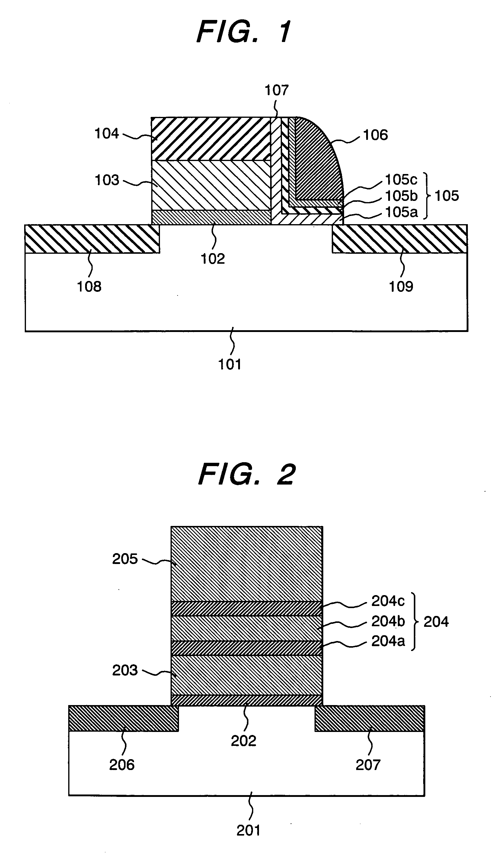
[0033] A first embodiment of the present invention will be described. This embodiment relates to a method of production that uses a high concentrated ozone for forming a silicon oxide film on top of the silicon oxide film, in a MONOS memory having a split gate construct utilizing self-alignment. FIG. 1 is a cross-sectional view of a nonvolatile memory cell according to a first embodiment of the present invention. Actually, in the upper part of the figure is present wiring, but it is omitted in this figure. The memory cell comprises two MOS transistors, including a p type well region 101 provided on a silicon substrate, an n type diffusion layer to be a source region 108, and an n type diffusion layer to be a drain region 109. The selective MOS transistor includes a silicon oxide film to be a gate insulating film 102, an n type poly-crystal Si film to be a selective gate electrode 103, and an insulating film 104 formed on top of the gate electrode. The memory MOS transistor has an in...

embodiment 2

[0050] Next, a second embodiment of the present invention will be set forth with reference to FIG. 2. This embodiment relates to a method of production that uses high-concentration ozone oxidation in forming a silicon oxide film on top of a silicon nitride film, in a floating gate type nonvolatile memory.

[0051]FIG. 2 is a cross-sectional view of a nonvolatile memory cell according to a second embodiment of the present invention. Actually, wiring is present in the upper part of the drawing, but is omitted in this figure. The memory cell includes a semiconductor substrate having a source region 206 and a drain region 207 that are formed by ion implantation and a tunneling silicon oxide film 202 formed on the channel between the source-drain regions. A floating gate electrode 203 comprised of poly-silicon is formed thereon. After formation of an interlayer insulating film 204 thereon, a control gate electrode 205 comprised of poly-silicon is formed thereon. The interlayer insulating f...


PUM


Abstract

Conventionally, a MONOS type nonvolatile memory is fabricated by subjecting a silicon nitride film to ISSG oxidation to form a top silicon oxide film of ONO structure. If the ISSG oxidation conditions are severe, repeats of programming / erase operation cause increase of interface state density (Dit) and electron trap density. This does not provide a sufficient value of the on current, posing a problem in that the deterioration of charge trapping properties cannot be suppressed. For the solution to the problem, the silicon nitride film is oxidized by means of a high concentration ozone gas to form the top silicon oxide film.

Description

CLAIM OF PRIORITY [0001] The present application claims priority from Japanese application JP 2004-168325, filed on Jun. 7, 2004, the content of which is hereby incorporated by reference into this application. BACKGROUND OF THE INVENTION [0002] 1. Field of the Invention [0003] The present invention relates in general to nonvolatile semiconductor storage devices (nonvolatile memories) capable of electrical programming and erase operation and methods of manufacturing the same. More in particular, it relates to a nonvolatile semiconductor storage device having a stacked structure of a silicon oxide film and a silicon nitride film and a method of manufacturing the same. [0004] 2. Description of the Related Art [0005] The nonvolatile semiconductor memory devices (nonvolatile memories) having a stacked structure possessing a silicon oxide film on top of a silicon nitride film can roughly classified into two systems: one is a system that uses a non-conductive charge trap film; and the othe...

Claims


Application Information

Patent Timeline
Patent Type & Authority Applications(United States)
IPC IPC(8): H01L21/28H01L21/336H01L27/10H01L21/8238H01L21/8247H01L27/115H01L29/423H01L29/51H01L29/788H01L29/792
CPCH01L21/28282H01L29/42344H01L29/513H01L29/792H01L29/40117
Inventor HAMAMURA, HIROTAKAMINE, TOSHIYUKIYOKOYAMA, NATSUKI
Owner RENESAS ELECTRONICS CORP
Why Eureka
Try Eureka