

Structure of TFT electrode for preventing metal layer diffusion and manufacturing method therefor
a technology of tft electrodes and electrode structures, which is applied in the direction of coupling device details, coupling device connections, transistors, etc., can solve the problems of chemical vapor depositing machines being affected by the environment, film quality formation can be easily affected by previously formed films, and affect the characteristics of tft, so as to reduce the risk of metallic ion contamination, prevent metal diffusion, and reduce the effect of processing environmen
- Summary
- Abstract
- Description
- Claims
- Application Information
AI Technical Summary
Benefits of technology
Problems solved by technology
Method used
Image

Examples
Embodiment Construction
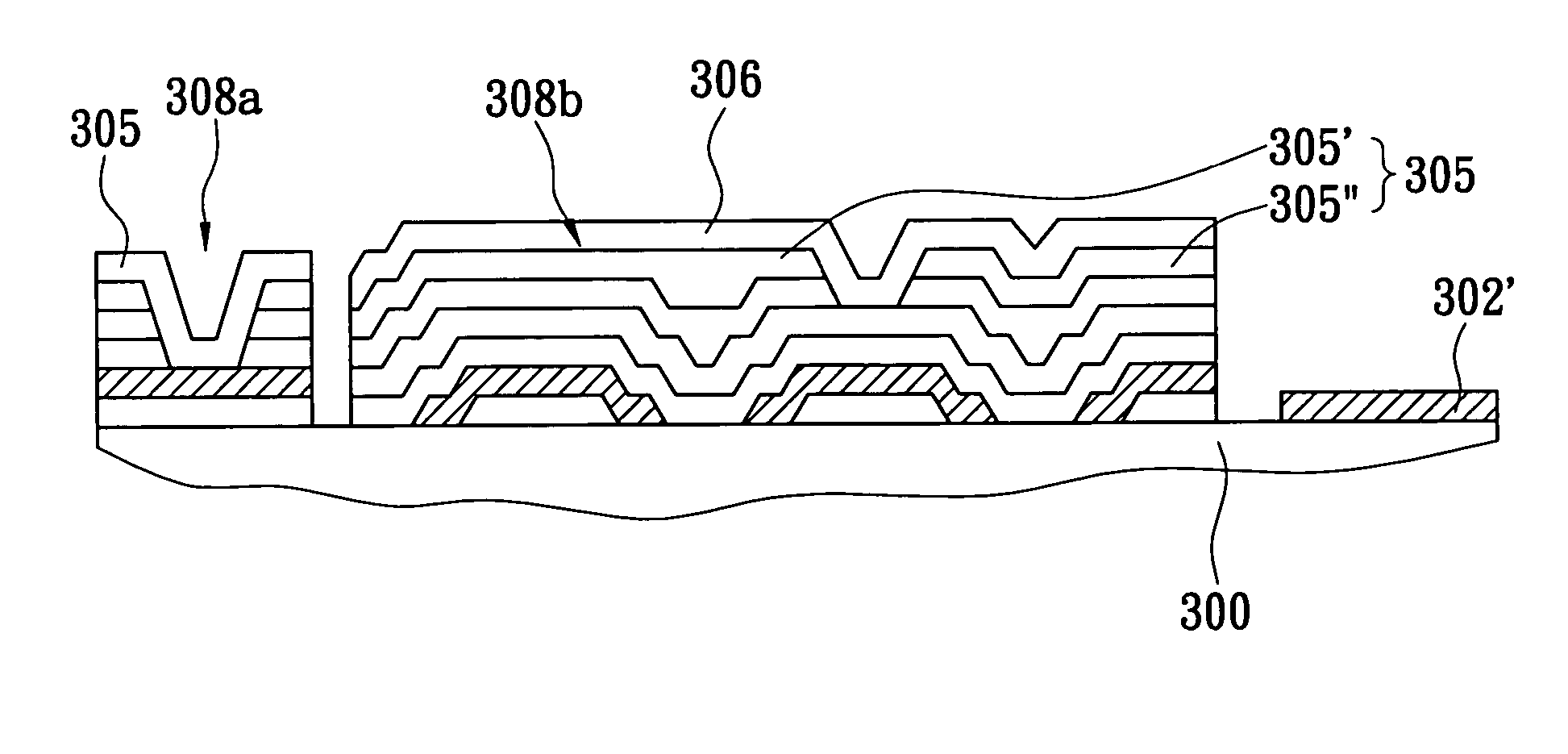
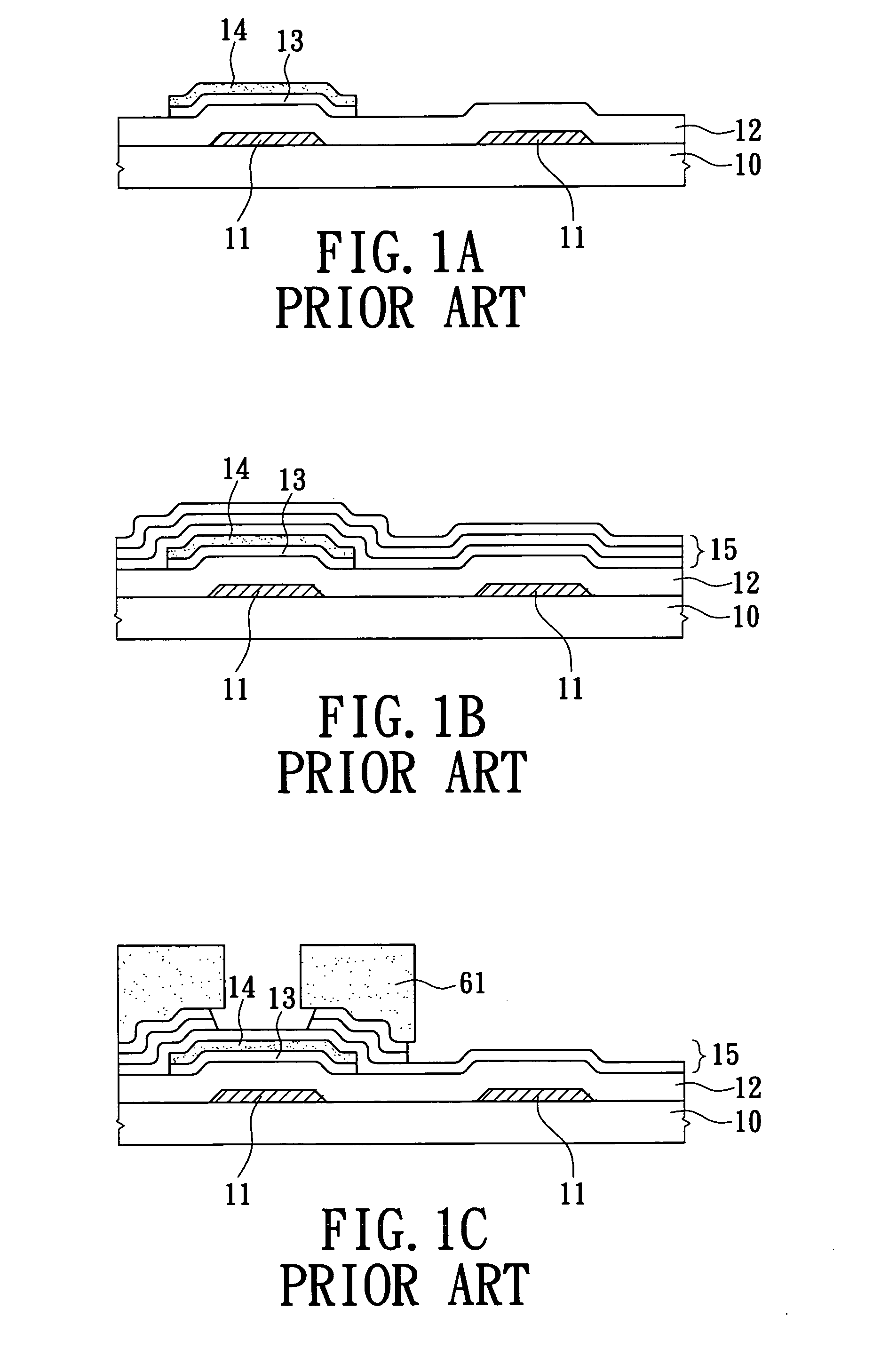
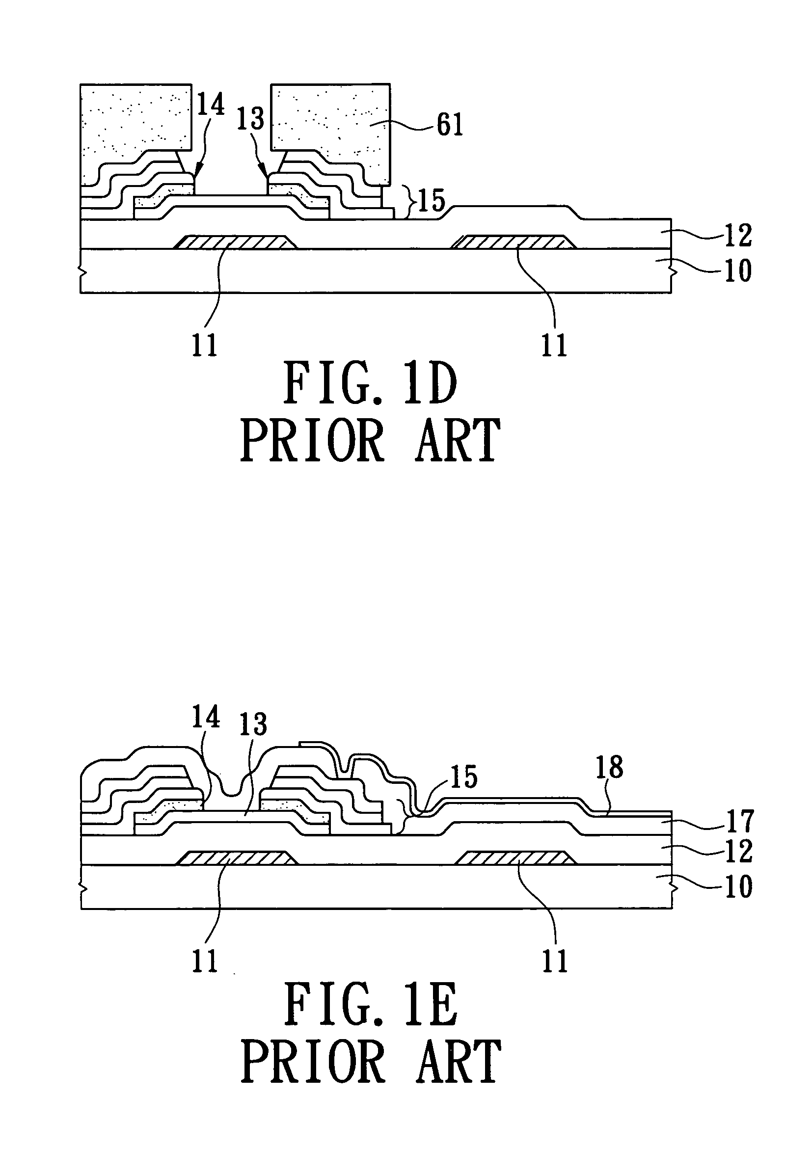
[0024] The invention provides a TFT electrode structure and its manufacturing process that can prevent metal diffusion, in particular copper metal diffusion, to an adjacent insulating layer during the manufacture of the TFT, so that current leakage and resulting poor conductivity problems can be improved.
[0025] In the TFT manufacturing process, the invention forms the pixel transparent electrode after the gate electrode metal so that the pixel transparent electrode can be used as a metallic ion barrier layer of the gate electrode metal. Due to its conduction property, the transparent electrode can prevent metallic ions from diffusing to the insulating layer and active layer at high temperature. Further, the conventional method uses an insulating layer formed by a high-temperature chemical vapor deposition method. In contrast, the pixel transparent electrode of the invention can be formed by a low-temperature physical vapor deposition method, which is affected less by the processing...
PUM
| Property | Measurement | Unit |
|---|---|---|
| transparent | aaaaa | aaaaa |
| conductive | aaaaa | aaaaa |
| dielectric | aaaaa | aaaaa |
Abstract
Description
Claims
Application Information