Electron emission apparatus comprising electron-emitting devices, image forming apparatus and voltage application apparatus for applying voltage between electrodes

an electron emission and electrode technology, applied in the direction of instruments, discharge tubes, luminescent screen devices, etc., can solve the problems of external resistors, inability to provide satisfactory solutions, and damage to electric discharges, so as to improve the electric connection, reduce the number of electrode segments short-circuited by the second member, and facilitate short-circuite

Inactive Publication Date: 2005-12-15
CANON KK
View PDF36 Cites 26 Cited by
  • Summary
  • Abstract
  • Description
  • Claims
  • Application Information

AI Technical Summary

Benefits of technology

[0034] When the supporting member includes a first member having a first electroconductivity and electrically connected to said electrode and a second member having a second electroconductivity arranged at the site of electric connection of the supporting member and the electrode to improve the electric connection and bridges at least two of the electrode segments of the electrode, the electrode segments can become easily short-circuited by the electrically highly conductive second member. This problem can be dissolved by electrically connecting the supporting member to some of the electrode segments at positions abutting the latter whereas it is electrically insulated from the rest of the electrode segments. With this arrangement, the number of electrode segments short-circuited by the second member can be reduced. Preferably, the supporting member is electrically connected to only one of the electrode segments at a position where they but each other. More specifically, this arrangement can be realized by using an electrically conductive adhesive agent for the electric connection and a dielectric adhesive agent for the electric insulation. With this arrangement, the first electroconductivity may be such that the short-circuiting among the plurality of electrode segments can be effectively suppressed below a permissible level. While the first electroconductivity may be selected to be low from the viewpoint of suppressing the power consumption rate of the supporting member, the effect of suppressing the short-circuiting and that of reducing the possible electric charge may also have to be taken into consideration.

Problems solved by technology

An electric discharge destruction can occur when a large electric current flows through certain spots of the electron source to generate heat that destructs the electron-emitting devices located there or instantaneously raise the voltage being applied to some of the electron-emitting devices to consequently destruct them.
However, such a measure by turn gives rise to another problem when a large number of electron-emitting devices are arranged in rows and columns, for example in 500 rows and 1,000 columns, and connected to a matrix wiring system so that they are driven sequentially on a line by line basis in such a way that as many as 1,000 devices are activated simultaneously.
Thus, the arrangement of an external resistor that is connected in series does not provide any satisfactory solution if it can dissolve the problem of uneven brightness.

Method used


Image

  • Electron emission apparatus comprising electron-emitting devices, image forming apparatus and voltage application apparatus for applying voltage between electrodes
  • Electron emission apparatus comprising electron-emitting devices, image forming apparatus and voltage application apparatus for applying voltage between electrodes
  • Electron emission apparatus comprising electron-emitting devices, image forming apparatus and voltage application apparatus for applying voltage between electrodes

Examples


example 1

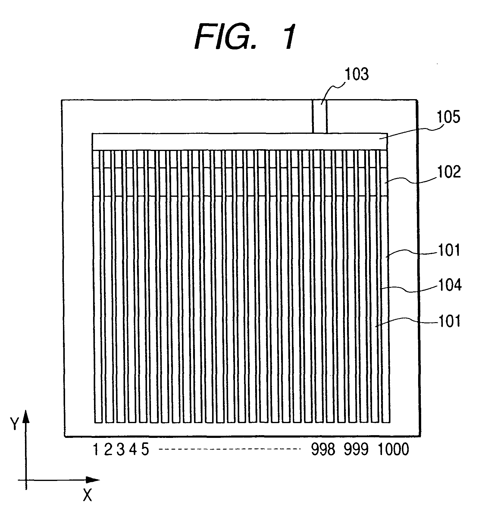
[0163] An image-forming apparatus comprising electron-emitting devices and having a configuration as described earlier by referring to FIG. 17 was prepared. The multiple-device electron source arranged on the rear plate of the apparatus was an SCE electron source (as will be described in greater detail hereinafter) provided with a matrix wiring arrangement as shown in FIG. 3. The electron source was so designed that 1,000 devices connected by a common wire were line-sequentially driven to operate. The electron source had a total of 1,000×500 electron emitting spots. On the other hand, the face plate of the apparatus was produced by forming uniformly an ITO film on a glass substrate, which ITO film was then divided into stripe-shaped segments (101) at a pitch of 230 μm (for 1,000 lines) by photolithography and bundled together at an end thereof by way of a resistor of 100 MQ (a patterned NiO film (102)) so that a high voltage may be applied via a terminal 103.

[0164] Then, referring ...

example 2

(The Use of Divided and Isolated Metal Back Segments of Al)

[0195] In this example, electroconductive black stripes (BSs) (1001) (containing carbon by 60% and water glass by 40% in a dispersed state) were formed on the glass substrate of the face plate by screen printing as shown in FIG. 15. Each of the stripes had a width of 100 μm and a thickness of 10 μm. The stripes were arranged at a pitch of 230 μm. The resistance of the stripes was 150 Ω / □.

[0196] Thereafter, stripes of RuO2 (1002) were formed as high resistance body by printing. Each of them showed a width of 100 μm, a length of 750 μm and an electric resistance of 10 MΩ. Then, R, G and B stripes were formed to fill the gaps among the BSs to a thickness of 10 μm by applying respective fluorescers P22 normally used for CRTs and baking the materials. Subsequently, a metal back of Al (1003) was formed by firstly producing an acrylic resin layer by dipping and then an Al layer to a thickness of 1,000 angstroms by evaporation an...

example 3

(The Use of Oblique Al Evaporation)

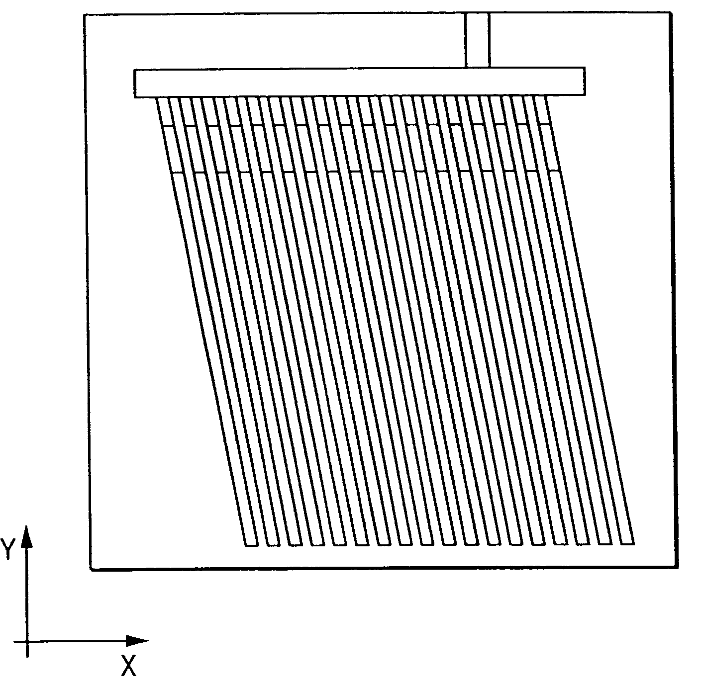
[0200] In this example, after forming a resin layer by dipping as in Example 2, an Al layer was formed by means of oblique Al evaporation as shown in FIGS. 16A and 16B. In FIGS. 16A and 16B, there are shown a fluorescent body 1105, a glass substrate 1106 of the face plate and an Al film 1107 formed by evaporation.

[0201] The BSs 1101 were made to show a height of 25 μm to produce a shadow of an Al beam 1102 as shown in FIG. 16B. Isolated segment stripes of Al film 1107 were formed by causing an Al beam to obliquely strike the face plate. After baking, it was confirmed that most (more than 90%) of the devices were electrically isolated for each line by more than 100 MΩ and then the prepared face plate was hermetically bonded to a rear plate. The devices were subjected to an activation process and then tested for the resistance against electric discharges as in Example 1 to find out a remarkable improvement as compared with a specimen comprising no...


PUM


Abstract

An electron emission apparatus can effectively suppress the adverse effect of electric discharges that can take place between the oppositely disposed electrodes of the apparatus to which a high voltage is applied by dividing the electrode adapted to have a higher electric potential into segments in order to reduce the electrostatic capacitance between the electrodes. In the case of an electron emission apparatus comprising electron-emitting devices, said plurality of electron-emitting devices are disposed such that the direction along which those that can be driven simultaneously are arranged is not parallel with the direction along which the electrode is divided into the electrode segments in order to reduce the variable range of the electric current that can flow in the segments.

Description

BACKGROUND OF THE INVENTION [0001] 1. Field of the Invention [0002] This invention relates to an electron emission apparatus comprising electron-emitting devices, an image-forming apparatus and a voltage application apparatus for applying a voltage between electrodes. [0003] 2. Related Background Art [0004] Known electron emission apparatus include image-forming apparatus such as an electron-beam display panel realized by arranging in parallel an electron source substrate carrying thereon a large number of cold cathode electron-emitting devices, a metal back or transparent electrode for accelerating electrons emitted from the electron-emitting devices and an anode substrate provided with a fluorescent body and evacuating the inside. An image-forming apparatus comprising field emission type electron-emitting devices is described in I. Brodie, “Advanced technology: flat cold-cathode CRT's”, Information Display, 1 / 89, 17 (1989). An image-forming apparatus comprising surface conduction ...

Claims


Application Information

Patent Timeline
Patent Type & Authority Applications(United States)
IPC IPC(8): H01J31/12H01J1/46H01J29/08H01J29/28H01J29/86H01J29/87
CPCH01J29/085H01J29/28H01J29/864H01J2329/863H01J2201/3165H01J2329/8625H01J31/127
Inventor HARA, TOSHITAMIMIYAZAKI, KAZUYAYAMANO, AKIHIKO
Owner CANON KK
Why Eureka
Try Eureka