
Advanced low dielectric constant barrier layers

a dielectric constant and barrier layer technology, applied in the direction of chemical vapor deposition coating, semiconductor/solid-state device details, coatings, etc., can solve the problems of short circuit formation, difficult etching of copper and achieving precise patterns, and failure of devices,

Inactive Publication Date: 2005-12-15
APPLIED MATERIALS INC
View PDF99 Cites 55 Cited by
  • Summary
  • Abstract
  • Description
  • Claims
  • Application Information

AI Technical Summary

Benefits of technology

[0012] Aspects of the invention generally provide a method for depositing a phosphorus doped barrier layer material having a low dielectric constant. In one aspect, the invention provides a method for processing a substrate including depositing a barrier layer on the substrate by introducing into a processing chamber a processing gas comprising an oxygen-free organosilicon compound, a phosphorus containing gas, and hydrogen, wherein the oxygen-free organosilicon compound has the formula SiHa(CH3)b(C6H5)c, and a is 0 to 3, b is 0 to 3, and c is 1 to 4 and reacting the processing gas to deposit the barrier layer, wherein the barrier layer has a dielectric constant less than 5 and depositing a dielectric layer adjacent the barrier layer, wherein the dielectric layer comprises silicon, oxygen, and

Problems solved by technology

One difficulty in using copper in semiconductor devices is that copper is difficult to etch and achieve a precise pattern.
Etching with copper using traditional deposition / etch processes for forming vertical and horizontal interconnects has been less than satisfactory.
However, low k dielectric materials are often porous and susceptible to interlayer diffusion of conductive materials, such as copper, and moisture, both of which can result in the formation of short-circuits and device failure.

Method used


Image

  • Advanced low dielectric constant barrier layers
  • Advanced low dielectric constant barrier layers
  • Advanced low dielectric constant barrier layers

Examples


Embodiment Construction

[0019] The words and phrases used herein should be given their ordinary and customary meaning to one skilled in the art unless otherwise further defined. The following deposition processes are described as though used in the 300 mm Producer™ dual deposition station processing chamber (Commercially available from Applied Materials, Inc., of Santa Clara, Calif.), and should be interpreted accordingly; for example, flow rates are total flow rates and should be divided by two to describe the process flow rates at each deposition station in the chamber. Additionally, it should be noted that the respective parameters may be modified to perform the plasma processes in various chambers and for different substrate sizes, such as for 200 mm substrates.

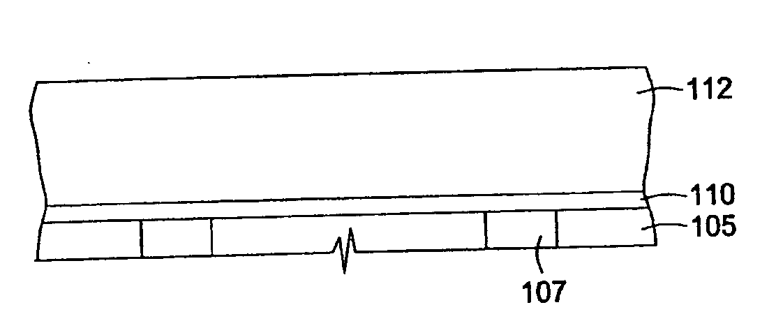
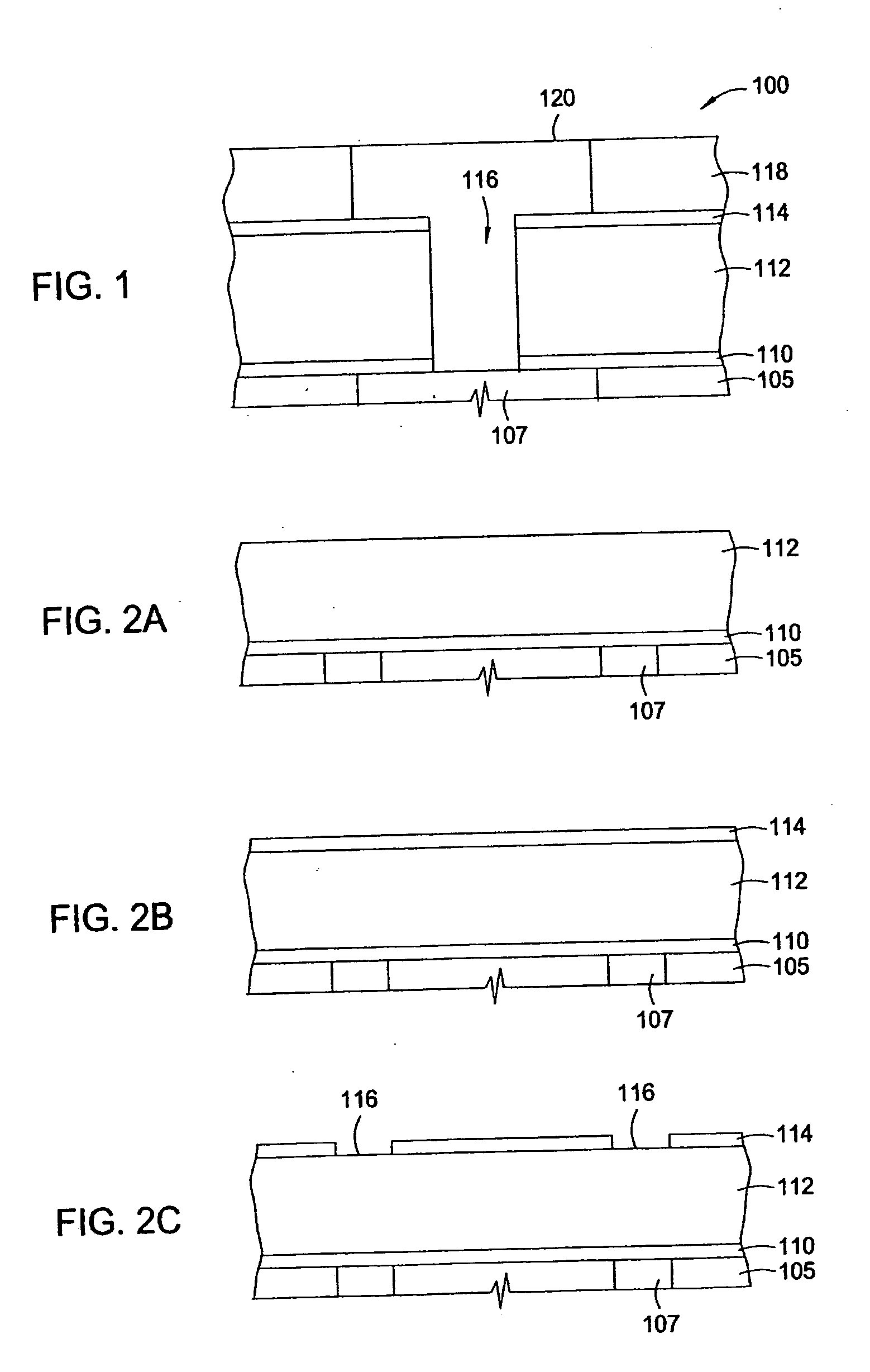
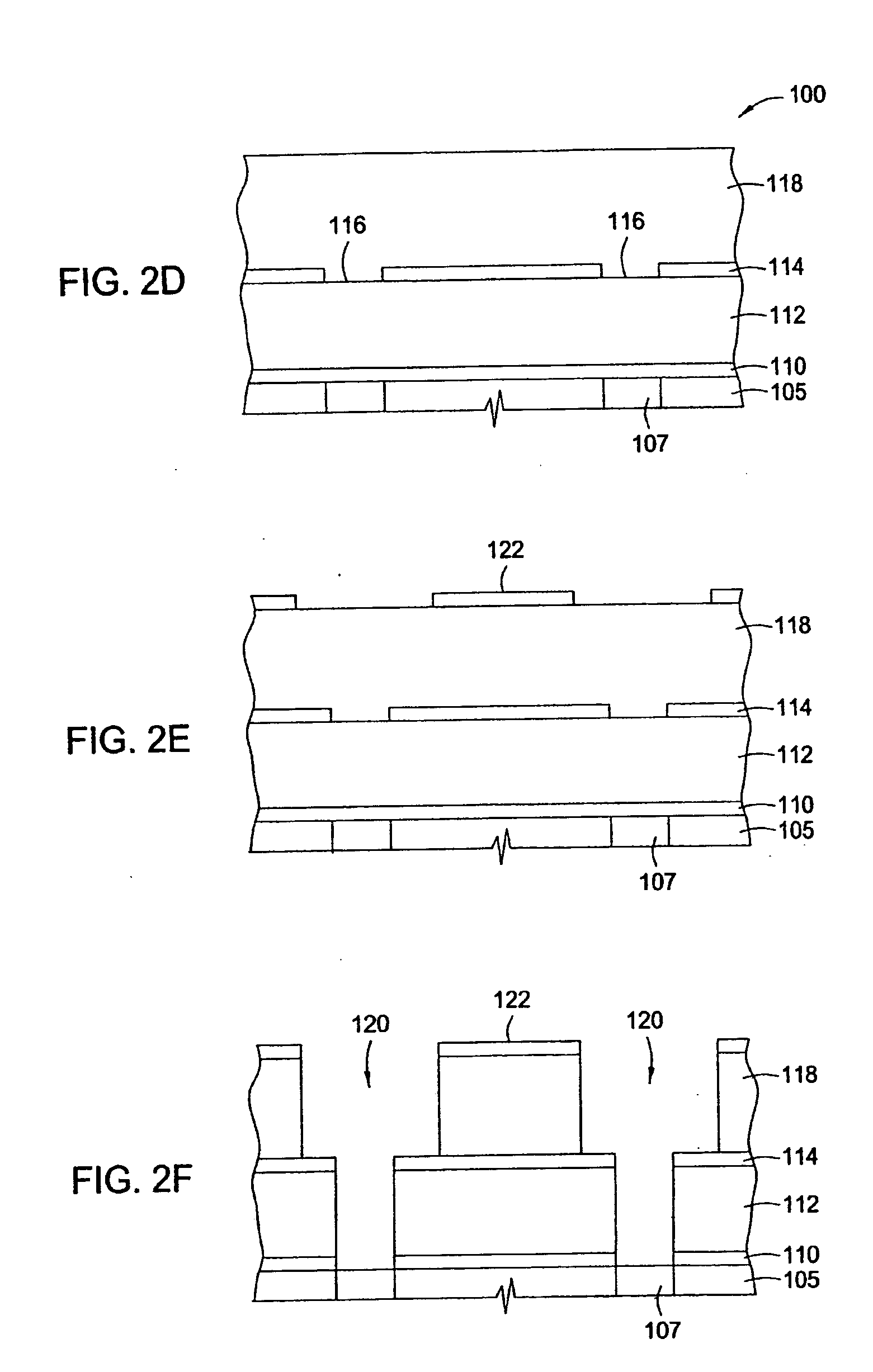
[0020] Aspects of the invention described herein refer to methods and compounds for depositing a phosphorus doped silicon carbide (SiCP) barrier layer material having a low dielectric constant, such as a dielectric constant of about 5 or less. ...


PUM

PropertyMeasurementUnit
Percent by atomaaaaaaaaaa

Abstract

Methods are provided for depositing a doped barrier layer material having a low dielectric constant. In one aspect, the invention provides a method for processing a substrate including depositing a barrier layer on the substrate by introducing a processing gas comprising an organosilicon compound, at least one dopant containing gas, hydrogen gas, and, optionally, an inert gas into a processing chamber, reacting the processing gas to deposit the barrier layer, and depositing a first dielectric layer adjacent the barrier layer. The organosilicon compound may comprise a phenylsilane containing compound or an aliphatic organosilicon compound. The processing gas may further comprise an oxygen containing compound, a nitrogen containing compound, or both.

Description

CROSS-REFERENCE TO RELATED APPLICATIONS [0001] This application claims benefit of U.S. Provisional Patent Application Ser. No. 60 / 575,663, filed May 28, 2004, which is herein incorporated by reference.BACKGROUND OF THE DISCLOSURE [0002] 1. Field of the Invention [0003] The invention relates to the fabrication of integrated circuits, more specifically to a process for depositing dielectric layers on a substrate, and to the structures formed by the dielectric layer. [0004] 2. Description of the Related Art [0005] Semiconductor device geometries have dramatically decreased in size since such devices were first introduced several decades ago. Since then, integrated circuits have generally followed the two year / half-size rule (often called Moore's Law), which means that the number of devices that will fit on a chip doubles every two years. Today's fabrication plants are routinely producing devices having 0.35 μm and even 0.18 μm feature sizes, and tomorrow's plants soon will be producing...

Claims


Application Information

Patent Timeline
IPC IPC(8): C23C16/32C23C16/505C23C16/56H01L21/312H01L21/469H01L21/768H01L23/532
CPCC23C16/325C23C16/505C23C16/56H01L21/3121H01L21/76801H01L21/7681H01L23/53295H01L21/76826H01L21/76828H01L21/76829H01L21/76835H01L23/5329H01L21/76825H01L2924/0002H01L21/02304H01L21/02126H01L21/02167H01L21/02274H01L2924/00
Inventor NGUYEN, SON VANM'SAAD, HICHEMKIM, BOK HOEN
Owner APPLIED MATERIALS INC
Learn More