Composition for preparing organic insulating film and organic insulating film prepared from the same

a technology of which is applied in the field of composition for preparing organic insulating film and organic insulating film, can solve the problems of inability to replace inorganic insulating film, inability to achieve the effect and inability to achieve the effect of achieving the effect of improving the electrical performance of the transistor

Inactive Publication Date: 2005-12-22
SAMSUNG ELECTRONICS CO LTD
View PDF2 Cites 44 Cited by
  • Summary
  • Abstract
  • Description
  • Claims
  • Application Information

AI Technical Summary

Benefits of technology

[0010] Therefore, the present invention has been made in view of the above problems of the related art, and it is an object of the present invention to provide a composition for preparing an organic insulating film having chemical resistance to organic s

Problems solved by technology

However, these inorganic oxide materials do not have a significant advantage over conventional silicon materials in terms of processing.
However, since these organic insulating films exhibit unsatisfactory device characteristics over inorganic insulating films, they are unsu

Method used


Image

  • Composition for preparing organic insulating film and organic insulating film prepared from the same
  • Composition for preparing organic insulating film and organic insulating film prepared from the same
  • Composition for preparing organic insulating film and organic insulating film prepared from the same

Examples


example 1

Fabrication of an Organic Thin Film Transistor by Using a Monomer Containing an Epoxide Group as a Functional Group

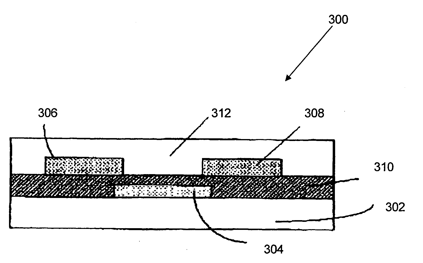
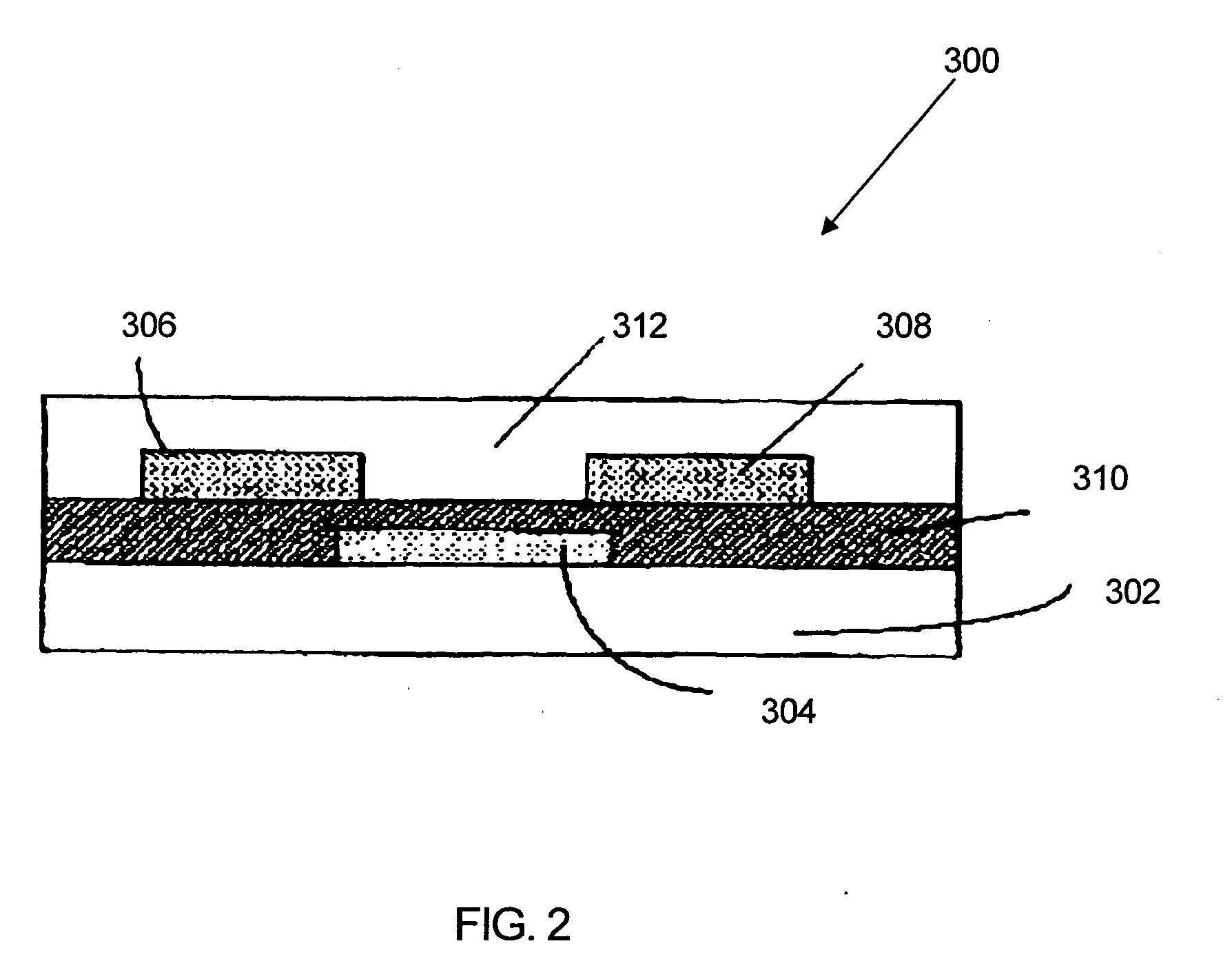
[0043] In this example, a bottom-contact organic thin film transistor was fabricated. First, Al was deposited on a washed glass substrate by a vacuum deposition technique to form a gate electrode having a thickness 1,500 Å. The composition prepared in Preparative Example 1 was then spin-coated on the gate electrode to a thickness of 5,000 Å at 4,000 rpm, prebaked at 100° C. for 5 minutes, irradiated by UV light at 600 W for 10 minutes, and baked at 100° C. for 1 hour to prepare the resulting organic insulating film. Next, Au was deposited on the organic insulating film to a thickness of 1,000 Å, and was subjected to a photolithographic process to form an Au electrode pattern. Pentacene was deposited on the Au electrode pattern to a thickness of 1,000 Å by organic molecular beam deposition (OMBD) under a vacuum of 2×10⁻⁷ torr at a substrate temperature of 50° C. and a d...

example 2

Fabrication of an Organic Thin Film Transistor by Using a Monomer Containing a Radical-Polymerizable Group as a Functional Group

[0044] An organic thin film transistor was fabricated in the same manner as in Example 1, except that the composition prepared in Preparative Example 2 was used instead of the composition prepared in Preparative Example 1.

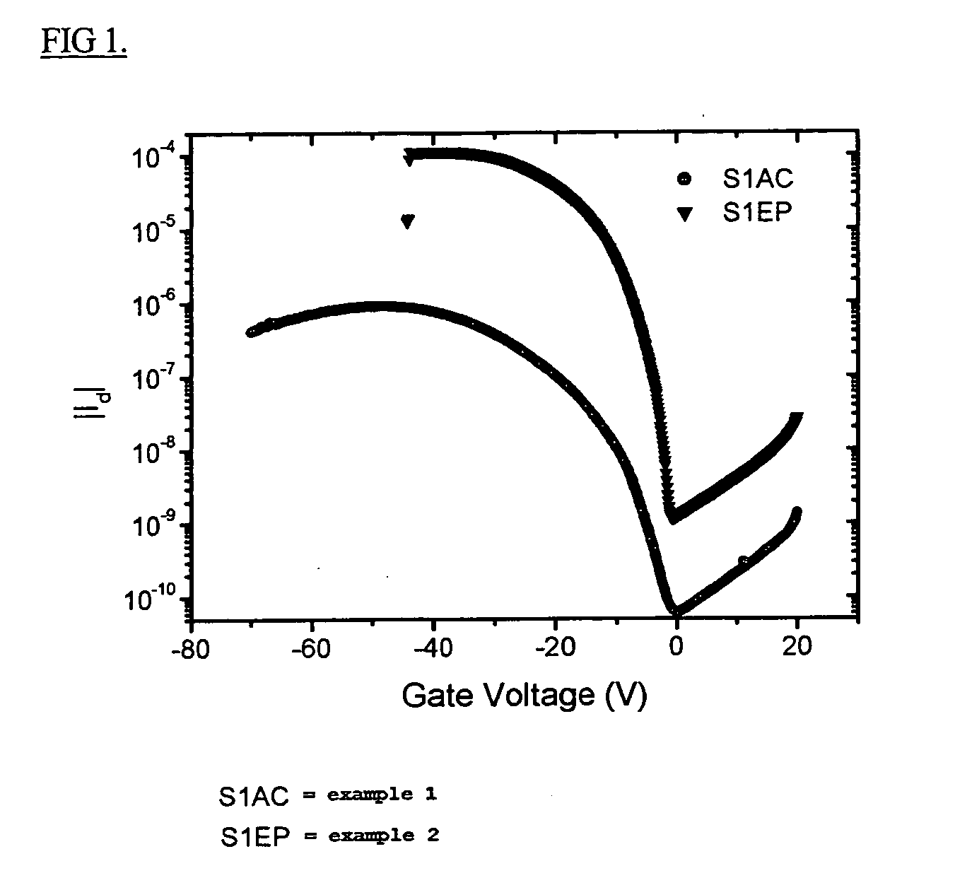
[0045] The current transfer characteristics of the devices fabricated in Examples 1 and 2 were measured using a KEITIHLEY semiconductor characterization system (4200-SCS), and curves were plotted (FIG. 1). The electrical properties of the devices calculated from the curves are shown in Table 1.


PUM

PropertyMeasurementUnit
Temperatureaaaaaaaaaa
Fractionaaaaaaaaaa
Percent by massaaaaaaaaaa

Abstract

A composition for preparing an organic insulating film. The composition includes a functional group-containing monomer, an initiator generating an acid or a radical upon light irradiation or heating, and a linear polymer. Further, an organic insulating film prepared from the composition. Since the organic insulating film has a crosslinked structure, it exhibits solvent resistance in subsequent processes. Further, when the organic insulating film is used to fabricate a transistor, it can improve the electrical properties of the transistor.

Description

BACKGROUND OF THE INVENTION [0001] This non-provisional application claims priority under 35 U.S.C. 119(a) on Korean Patent Application No. 200446177 filed on Jun. 21, 2004 which is herein expressly incorporated by reference. [0002] A. Field of the Invention [0003] The present invention relates to a composition for preparing an organic insulating film, and an organic insulating film prepared from the composition. More specifically, the present invention relates to a composition for preparing a crosslinked organic insulating film having chemical resistance to organic solvents used in subsequent processes after preparation of the organic insulating film, and an organic insulating film prepared from the composition. [0004] B. Description of the Related Art [0005] Since polyacetylenes as conjugated organic polymers exhibiting semiconductor characteristics were developed, organic semiconductors have been actively investigated as novel electrical and electronic materials in a wide variety...

Claims


Application Information

Patent Timeline
IPC IPC(8): H01L29/08H01L51/05
CPCC08L63/00G03F7/027G03F7/038H01L51/0052H01L51/052C08L2666/02H10K85/615H10K10/471C08G59/14C08G59/02C08J5/22
Inventor SHIN, JUNG HANLEE, TAE WOOLEE, SANG YOONPARK, HYUNG JUNG
Owner SAMSUNG ELECTRONICS CO LTD
Why Eureka
Try Eureka